Array substrate, display panel and display device

An array substrate and display device technology, applied in nonlinear optics, instruments, optics, etc., can solve the problems affecting the display panel image display effect, the display unit potential that affects the display area, and the high ion content at the edge of the digging area, ensuring that the The effect of image display effect, prolonging service life and reducing the probability of water vapor entering the liquid crystal cell

Pending Publication Date: 2018-12-21
XIAMEN TIANMA MICRO ELECTRONICS
View PDF6 Cites 10 Cited by
  • Summary
  • Abstract
  • Description
  • Claims
  • Application Information

AI Technical Summary

Problems solved by technology

[0003] Usually, after the hole-digging area is formed in the display area, the curing effect of the sealant around the hole-digging area is poor, resulting in high ion content at the edge of the hole-digging area, which affects the potential of the display unit in the display area, thereby affecting the image display effect of the display panel

Method used


Image

  • Array substrate, display panel and display device
  • Array substrate, display panel and display device
  • Array substrate, display panel and display device

Examples


Embodiment Construction

[0028] The present invention will be further described in detail below in conjunction with the accompanying drawings and embodiments. It should be understood that the specific embodiments described here are only used to explain the present invention, but not to limit the present invention. In addition, it should be noted that, for the convenience of description, only some structures related to the present invention are shown in the drawings but not all structures.

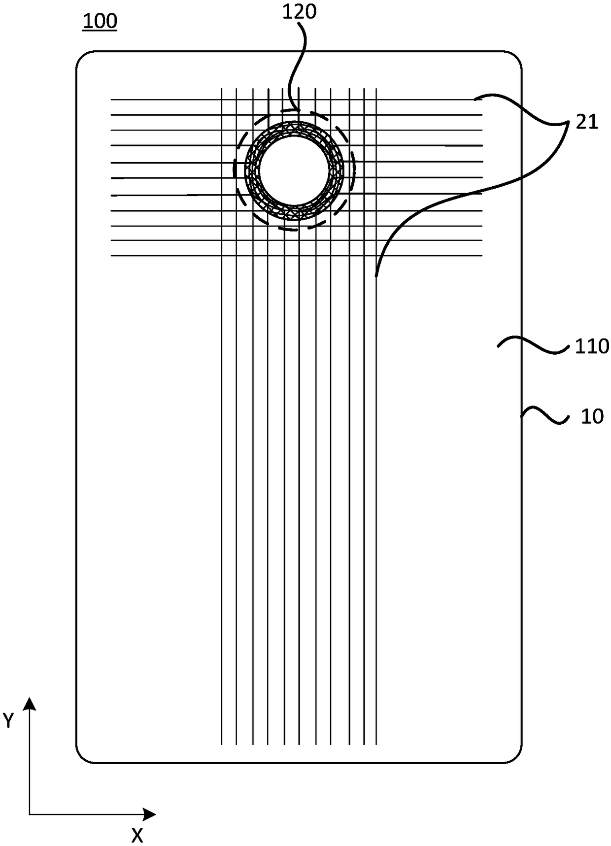
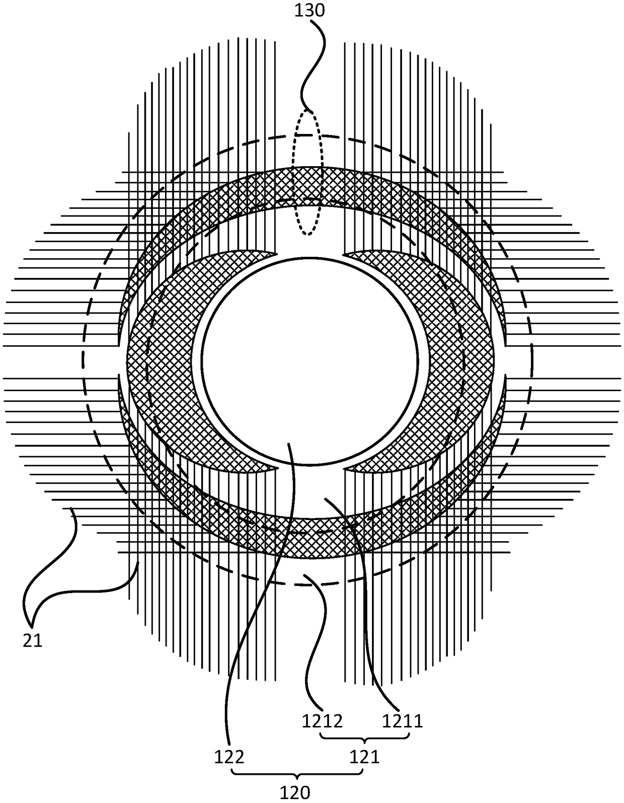
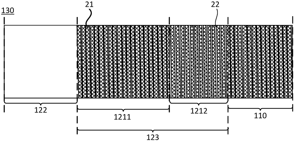
[0029] figure 1 A schematic plan view of an array substrate provided by an embodiment of the present invention, figure 2 for figure 1 A schematic diagram of a planar structure of the Central Africa display area, image 3 for figure 2 A schematic diagram of the planar structure of the 130 area. refer to Figure 1-Figure 3 , the array substrate 100 includes a display area 110 and at least one non-display area 120 ( figure 1 The number of the non-display area 120 is only exemplarily shown in 1), the display a...


PUM


Abstract

The present invention discloses an array substrate, a display panel and a display device. The array substrate comprises a display area and at least one non-display area, and the display area surroundsthe non-display area. The non-display area comprises a wiring area and a module arranging area. The array substrate comprises a substrate base plate and multiple signal lines, and the multiple signallines extend to the wiring area and surround the module arranging area. The multiple signal lines on the wiring area are also provided with frame glue. The wiring area comprises a first wiring area and a second wiring area, the inner edge of the first wiring area is contacted with the module arranging area, the second wiring area surrounds the first wiring area, the upright projection, on the substrate base plate, of the first wiring area and the second wiring area is located in the upright projection, on the substrate base plate, of the frame glue, and the outer edge of the second wiring area is contacted with the outer edge of the frame glue. The light transmittance of the first wiring area is less than the light transmittance of the second wiring area. The array substrate can improve the curing efficiency of the frame glue, so that the ion content is reduced, and the image display effect is improved.

Description

technical field [0001] The present invention relates to display technology, in particular to an array substrate, a display panel and a display device. Background technique [0002] With the development of display technology, in order to improve user experience, high screen-to-body ratio has gradually become an important development direction of display panels and display devices. The screen-to-body ratio can be understood as the ratio of the visible area of ​​the display panel to the total area of ​​the plane on which it is located. In order to increase the screen-to-body ratio, it is necessary to reduce the area occupied by the frame area of ​​the display panel, thereby reducing the area occupied by the non-display area. For this, holes can be dug in the display area, and the modules ( For example: the front camera on the mobile phone, the front flash, the earpiece, etc.) are set in the hole-digging area. [0003] Usually, after the hole-digging area is formed in the disp...

Claims


Application Information

Patent Timeline
Patent Type & Authority Applications(China)
IPC IPC(8): G02F1/1362G02F1/1339
CPCG02F1/1339G02F1/136286
Inventor 赖国昌
Owner XIAMEN TIANMA MICRO ELECTRONICS
Why Eureka
Try Eureka