A kind of manufacturing method of dbr flip chip
A flip-chip and manufacturing method technology, applied in semiconductor devices, electrical components, circuits, etc., can solve the problem that DBR flip-chip is not suitable for high-current and high-power use.
- Summary
- Abstract
- Description
- Claims
- Application Information
AI Technical Summary
Problems solved by technology
Method used
Image


Examples
Embodiment Construction
[0016] The specific embodiments of the present invention will be described in further detail below in conjunction with the drawings and embodiments. The following examples are used to illustrate the present invention, but not to limit the scope of the present invention.
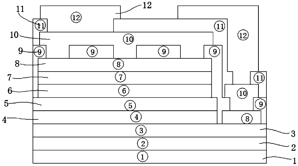
[0017] See Figure 1-2 , Is a DBR flip chip manufacturing method provided by the present invention, including the following steps: step one, fabricating an epitaxial layer; specifically, the step one includes: sequentially growing a buffer layer on the sapphire substrate 1 by MOCVD equipment 2. The N-GaN layer 3, the light emitting quantum well 4 and the P-GaN layer 5 complete the fabrication of the GaN-based LED epitaxial layer. Step two, etch N-type steps on the epitaxial layer structure to make the N-GaN in a bare state; step three, grow a reflective layer and a metal binding layer 8 on the surface of the epitaxial layer, respectively; step four, A DBR Bragg reflector layer 9 is grown on the DBR flip chip, ...
PUM
 Abstract
Description
Claims
Application Information
 - R&D Engineer
- R&D Manager
- IP Professional
- Industry Leading Data Capabilities
- Powerful AI technology
- Patent DNA Extraction
Browse by: Latest US Patents, China's latest patents, Technical Efficacy Thesaurus, Application Domain, Technology Topic.
© 2024 PatSnap. All rights reserved.Legal|Privacy policy|Modern Slavery Act Transparency Statement|Sitemap