Fabrication method of DBR flip chip

A flip-chip and manufacturing method technology, applied in electrical components, circuits, semiconductor devices, etc., can solve the problem that DBR flip-chip is not suitable for high-current and high-power use.

Active Publication Date: 2019-04-16
GUANGDONG DELI PHOTOELECTRIC
View PDF4 Cites 3 Cited by
  • Summary
  • Abstract
  • Description
  • Claims
  • Application Information

AI Technical Summary

Problems solved by technology

Under the conditions of high current and high power, the thin transparent metal conductive film is not enough to spread the current uniformly, so the traditional DBR flip chip is not suitable for high current and high power use

Method used


Image

  • Fabrication method of DBR flip chip
  • Fabrication method of DBR flip chip

Examples


Embodiment Construction

[0016] The specific implementation manners of the present invention will be further described in detail below in conjunction with the accompanying drawings and embodiments. The following examples are used to illustrate the present invention, but are not intended to limit the scope of the present invention.

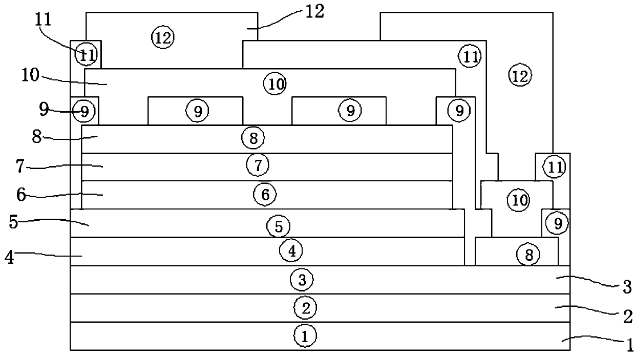
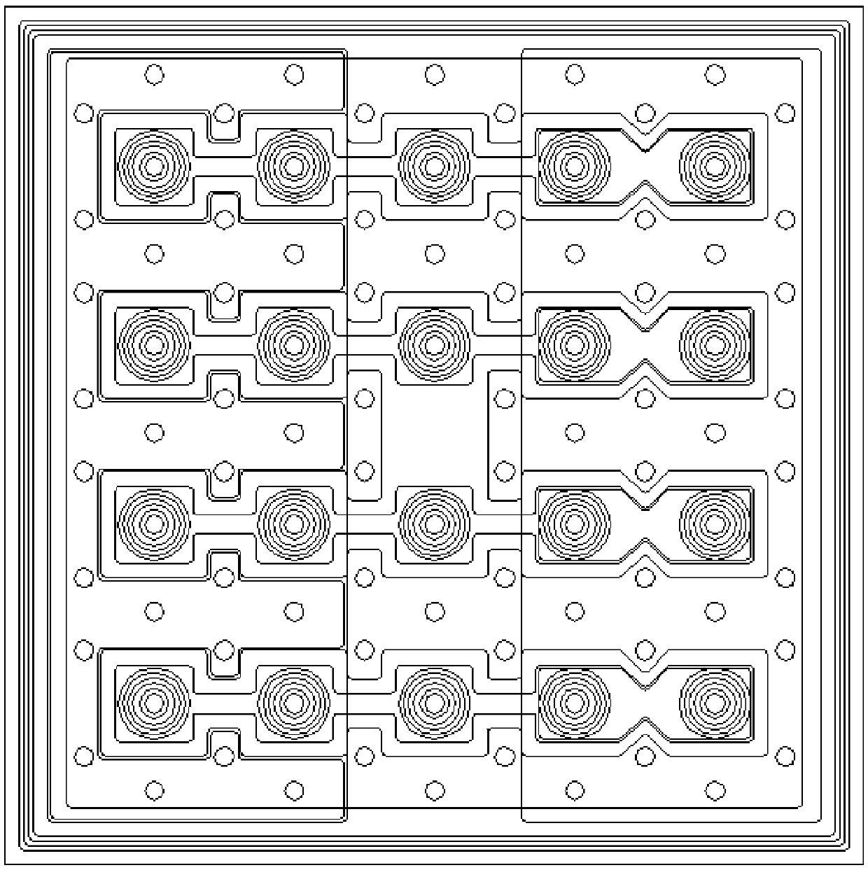
[0017] See Figure 1-2 , a DBR flip chip manufacturing method provided by the present invention, comprising the following steps: Step 1, making an epitaxial layer; specifically, Step 1 includes: sequentially growing a buffer layer on a sapphire substrate 1 by MOCVD equipment 2. N-GaN layer 3, light-emitting quantum well 4 and P-GaN layer 5, to complete the fabrication of GaN-based LED epitaxial layer. Step 2, etching an N-type step on the epitaxial layer structure, so that N-GaN is in a bare state; Step 3, growing a reflective layer and a metal binding layer 8 on the surface of the epitaxial layer; Step 4, Grow DBR Bragg reflector layer 9 on described DBR flip-chip, and ...


PUM


Abstract

The invention relates to a fabrication method of a DBR flip chip. The fabrication method comprises the following steps of 1, fabricating an epitaxial layer; 2, etching an N-type step on an epitaxial layer structure; 3, growing a reflection layer and a metal binding layer on a surface of the epitaxial layer; 4, growing a DBR layer on the DBR flip chip, and respectively P electrode conductive holesand N electrode conductive holes; and 5, evaporating a current expansion metal layer on the DBR layer according to the arrangement of the conductive holes, and allowing the P electrode conductive holeand the N electrode conductive hole to be connected. According to the fabrication method of the DBR flip chip, provided by the invention, the uniform current expansion can be ensured under the application condition of large current and large power, so that the DBR flip chip can be applied to a large-power condition.

Description

technical field [0001] The invention relates to the field of LED flip chips, in particular to a method for manufacturing a DBR flip chip. Background technique [0002] The traditional DBR flip-chip process is based on the front-mount chip process, and the DBR passivation layer is evaporated on the front of the front-mount chip as a reflective layer, and then the corresponding P-electrode conductive holes and N-electrode conductive holes are etched on the DBR layer. , and finally vapor-deposit P and N electrode layers on the surface of the DBR. The electrode layer respectively covers the P electrode conductive hole and the N electrode conductive hole in the DBR layer, and the chip is conducted downward by using the P and N electrode holes, thereby obtaining the effect of flip chip. Since the traditional flip chip uses a DBR reflector as the reflective layer, the area of ​​the current spreading metal layer between the light-emitting layer and the reflective layer should not b...

Claims


Application Information

Patent Timeline
IPC IPC(8): H01L33/38H01L33/46
CPCH01L33/387H01L33/46H01L2933/0016H01L2933/0025
Inventor 张洪安陈慧秋武杰易翰翔李玉珠
Owner GUANGDONG DELI PHOTOELECTRIC
Why Eureka
Try Eureka