Resonant cavity microarray high-efficiency light emitting diode chip

A technology of light-emitting diodes and resonant cavities, applied in electrical components, electric solid-state devices, circuits, etc., can solve the problems of increasing light extraction efficiency, external quantum efficiency, and low light extraction efficiency, so as to improve light extraction efficiency and solve the blocking effect , the effect of increasing the relative area ratio

Active Publication Date: 2021-01-22
BEIJING UNIV OF TECH
View PDF7 Cites 8 Cited by
  • Summary
  • Abstract
  • Description
  • Claims
  • Application Information

AI Technical Summary

Problems solved by technology

[0003] The object of the present invention is to propose a micro-array high-efficiency light-emitting diode chip based on a resonant cavity, which not only changes the internal light field distribution by using the resonant cavity structure, improves the light extraction efficiency of light from the upper surface of the chip, but also adopts the micro-array structure to make The relative area ratio of the surrounding side walls perpendicular to the upper surface is increased, effectively extracting the light emitted by the side walls, thereby increasing the light extraction efficiency and increasing its external quantum efficiency, so as to simultaneously solve the five problems existing in the above-mentioned traditional LEDs and ordinary LEDs. The problem of low light extraction efficiency of RCLED

Method used


Image

  • Resonant cavity microarray high-efficiency light emitting diode chip
  • Resonant cavity microarray high-efficiency light emitting diode chip
  • Resonant cavity microarray high-efficiency light emitting diode chip

Examples


Embodiment Construction

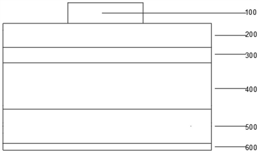
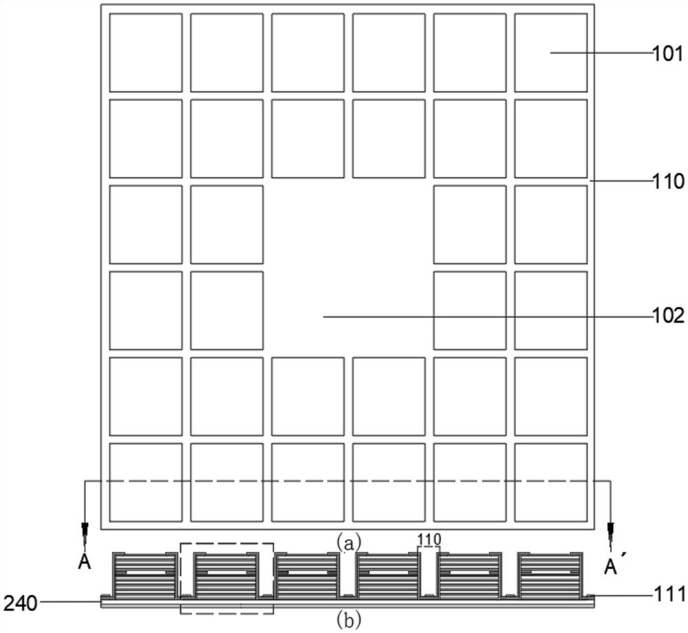
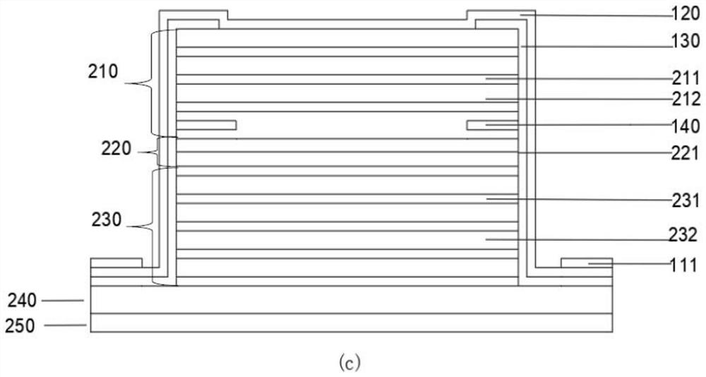
[0018] Such as figure 2 (b) The realization of the high-efficiency 650nm red light-emitting diode chip based on the resonant cavity microarray is as follows:

[0019] 1. Growth epitaxial wafer

[0020] On the N-type GaAs substrate 240, 30 pairs of N-doped lower Bragg mirrors 230 are epitaxially grown sequentially by metal-organic chemical vapor deposition (MOCVD), with a doping concentration of 10 18 cm -3 , wherein the high-refractive-index material 231 and the low-refractive-index material 232 are Al with a thickness of 46.6 nm and a refractive index of about 3.477. 0.5 Ga 0.5 As and AlAs with a thickness of 50.1 nm and a refractive index of about 3.112. Then grow non-doped resonant cavity 220 and active region 221, using three Ga 0.5 In 0.5 P / (Al 0.5 Ga 0.5 )In 0.5 The P multiquantum well is used as the light-emitting active region, and the thickness of the well and the barrier are both 5nm. Then there is a pair of P-type AlAs layers for lateral oxidation, with a...


PUM

PropertyMeasurementUnit
thicknessaaaaaaaaaa
thicknessaaaaaaaaaa
reflectanceaaaaaaaaaa

Abstract

The invention discloses a resonant cavity microarray high-efficiency light emitting diode chip, which belongs to the field of semiconductor photoelectrons. The resonant cavity microarray high-efficiency light emitting diode chip comprises a transparent conductive layer ITO, a SiO2 isolation layer, an upper Bragg reflector, a resonant cavity, a lower Bragg reflector, a current expansion upper electrode, a substrate, a lower electrode and a lateral oxide layer located above the resonant cavity. The resonant cavity contains an optical radiation active region. The upper Bragg reflector is composedof low-refractive-index material layers and high-refractive-index material layers which are alternately arranged, and the thicknesses of the low-refractive-index material layers and the high-refractive-index material layers are 1 / 4 of the wavelength of incident light. The lower Bragg reflector is composed of low-refractive-index material layers and high-refractive-index material layers which arealternately arranged, and the thicknesses of the low-refractive-index material layers and the high-refractive-index material layers are 1 / 4 of the wavelength of incident light. The light extraction efficiency of the light from the upper surface of the chip is improved, and the light emitted from the side wall can be effectively extracted, so that the light extraction efficiency is improved, the external quantum efficiency is improved, and the resonant cavity microarray high-efficiency light emitting diode chip is realized.

Description

technical field [0001] The invention relates to a resonant cavity-based microarray high-efficiency light-emitting diode chip, which belongs to the field of semiconductor optoelectronics. Background technique [0002] With the continuous improvement of the light efficiency of LED chips, the application of LEDs in the fields of optical fiber communication and lighting has become more and more extensive. The luminous efficiency of LED usually refers to external quantum efficiency, which is the product of internal quantum efficiency and light extraction efficiency. Although the use of quantum wells and heterojunctions to design the active region can make the internal quantum efficiency of LEDs close to the theoretical limit of 100%, the optimal light extraction efficiency of ordinary LEDs is around 2%. Its simple structure is as figure 1 As shown, it includes an upper electrode 100 , an upper confinement layer 200 , an active region 300 , a lower confinement layer 400 , a subs...

Claims


Application Information

Patent Timeline
Patent Type & Authority Applications(China)
IPC IPC(8): H01L33/10H01L33/14H01L33/36H01L27/15
CPCH01L27/156H01L33/105H01L33/36H01L33/14H01L33/10
Inventor 李建军杨启伟
Owner BEIJING UNIV OF TECH
Why Eureka
Try Eureka