A pcb metal hole embedded copper structure and its processing technology

A processing technology and metal hole technology, applied in the field of PCB metal hole copper embedded structure and its processing technology, can solve the problems of high cost of buried copper process, many embedded copper particles, slow speed, etc., to solve the defects of poor heat conduction and reduce processing cycle effect

Active Publication Date: 2020-08-25
厦门四合微电子有限公司
View PDF5 Cites 0 Cited by
  • Summary
  • Abstract
  • Description
  • Claims
  • Application Information

AI Technical Summary

Problems solved by technology

[0004] (1) The existing process is only manually inserted, which is slow and inefficient;
[0005] (2) There are too many copper particles embedded on a single PCB, and the cost of the buried copper process is too high
[0006] Therefore, the existing PCB board manufacturing process still needs to be improved and developed.

Method used


Image

  • A pcb metal hole embedded copper structure and its processing technology
  • A pcb metal hole embedded copper structure and its processing technology
  • A pcb metal hole embedded copper structure and its processing technology

Examples


Embodiment Construction

[0028] In order to make the above objects, features and advantages of the present invention more comprehensible, specific implementations of the present invention will be described in detail below in conjunction with the accompanying drawings.

[0029] The terms used herein in the description of the present invention are for the purpose of describing specific embodiments only, and are not intended to limit the present invention. As used herein, the term "and / or" includes any and all combinations of one or more of the associated listed items.

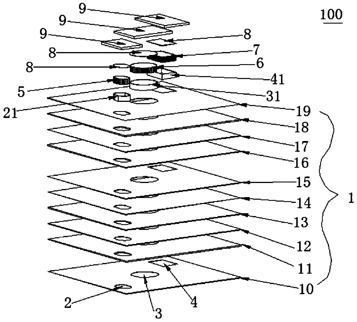
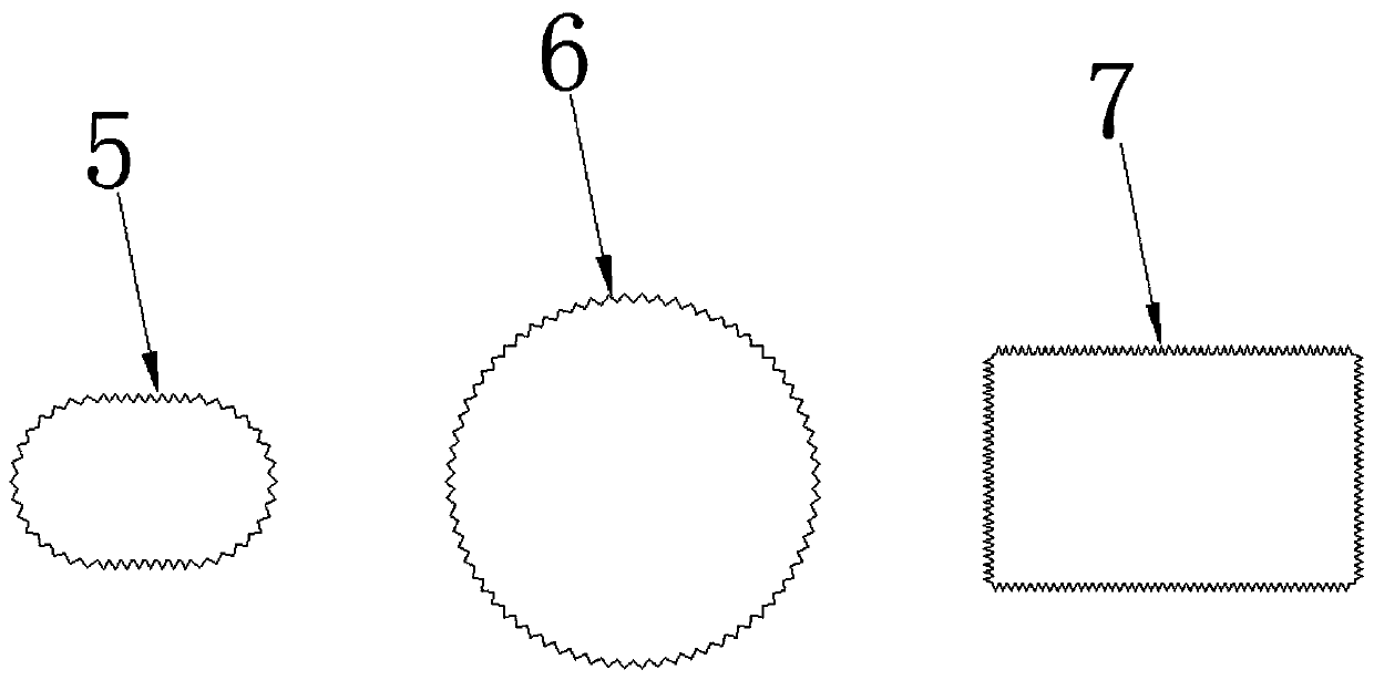
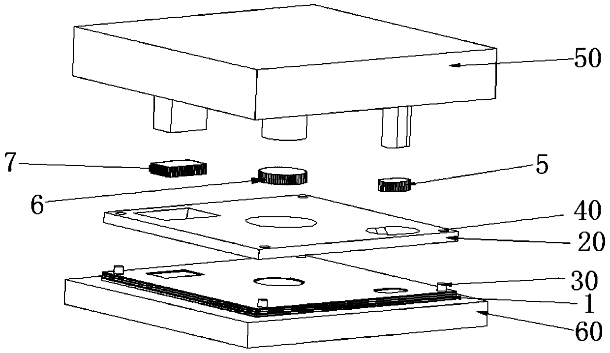
[0030] figure 1 It is an exploded view of a PCB metal hole copper embedded structure provided by an embodiment of the present invention. figure 2 is the invention figure 1 The top view of the first copper block, the second copper block, and the third through hole in . image 3 It is a schematic diagram of a PCB metal hole copper embedded structure processing technology provided by an embodiment of the present invention.

[0031] see...


PUM


Abstract

The invention discloses a PCB metal hole copper embedding structure. The structure comprises a PCB, a first through hole, a second through hole, a third through hole, a first copper block, a second copper block and a third copper block, wherein the first through hole, the second through hole and the third through hole respectively penetrate through the PCB, the first through hole is provided witha first electroless plating copper hole wall, the second through hole is provided with a second electroless plating copper hole wall, and the third through hole is provided with a third electroless plating copper hole wall; The circumferences of the first copper block, the second copper block and the third copper block are all provided with teeth. The first copper block is embedded into the firstthrough hole provided with the first electroless plating copper hole wall, the second copper block is embedded into the second through hole provided with the second electroless plating copper hole wall, and the third copper block is embedded into the third through hole provided with the third electroless plating copper hole wall. The invention further provides a processing technology of the PCB metal hole copper embedding structure, and other copper embedding modes except the copper embedding technology of the PCB are achieved.

Description

technical field [0001] The invention belongs to the technical field of circuit boards, and in particular relates to a copper-embedded PCB metal hole structure and a processing technology thereof. Background technique [0002] With the diversified development of product miniaturization and high power, the conventional multi-layer flat-panel PCB can no longer bear greater heat dissipation requirements, and the existing PCB buried copper process is relatively complicated, and both sides cannot be completely exposed on the surface. Embedded during processing, the processing cycle is relatively long. Moreover, in the existing PCB copper embedding process, the embedded copper can only be press-fitted in holes without metal walls, but not embedded in metal holes. [0003] Therefore, the existing PCB buried copper process has the following defects: [0004] (1) The existing process is only manually inserted, which is slow and inefficient; [0005] (2) There are too many copper pa...

Claims


Application Information

Patent Timeline
Patent Type & Authority Patents(China)
IPC IPC(8): H05K1/02H05K3/00
CPCH05K1/0204H05K3/0008H05K3/0094H05K2201/10416
Inventor 文明赵铁良张海方
Owner 厦门四合微电子有限公司
Why Eureka
Try Eureka