A wafer disc positioning method and device

A positioning method and a technology for predetermined positions, which are used in image data processing, instrumentation, computing, etc.

Active Publication Date: 2019-06-14
ZHEJIANG SUNNY OPTICAL CO LTD
View PDF8 Cites 3 Cited by
  • Summary
  • Abstract
  • Description
  • Claims
  • Application Information

AI Technical Summary

Problems solved by technology

[0006] Embodiments of the present invention provide a wafer positioning method and device to at least solve th

Method used


Image

  • A wafer disc positioning method and device
  • A wafer disc positioning method and device
  • A wafer disc positioning method and device

Examples


Embodiment 1

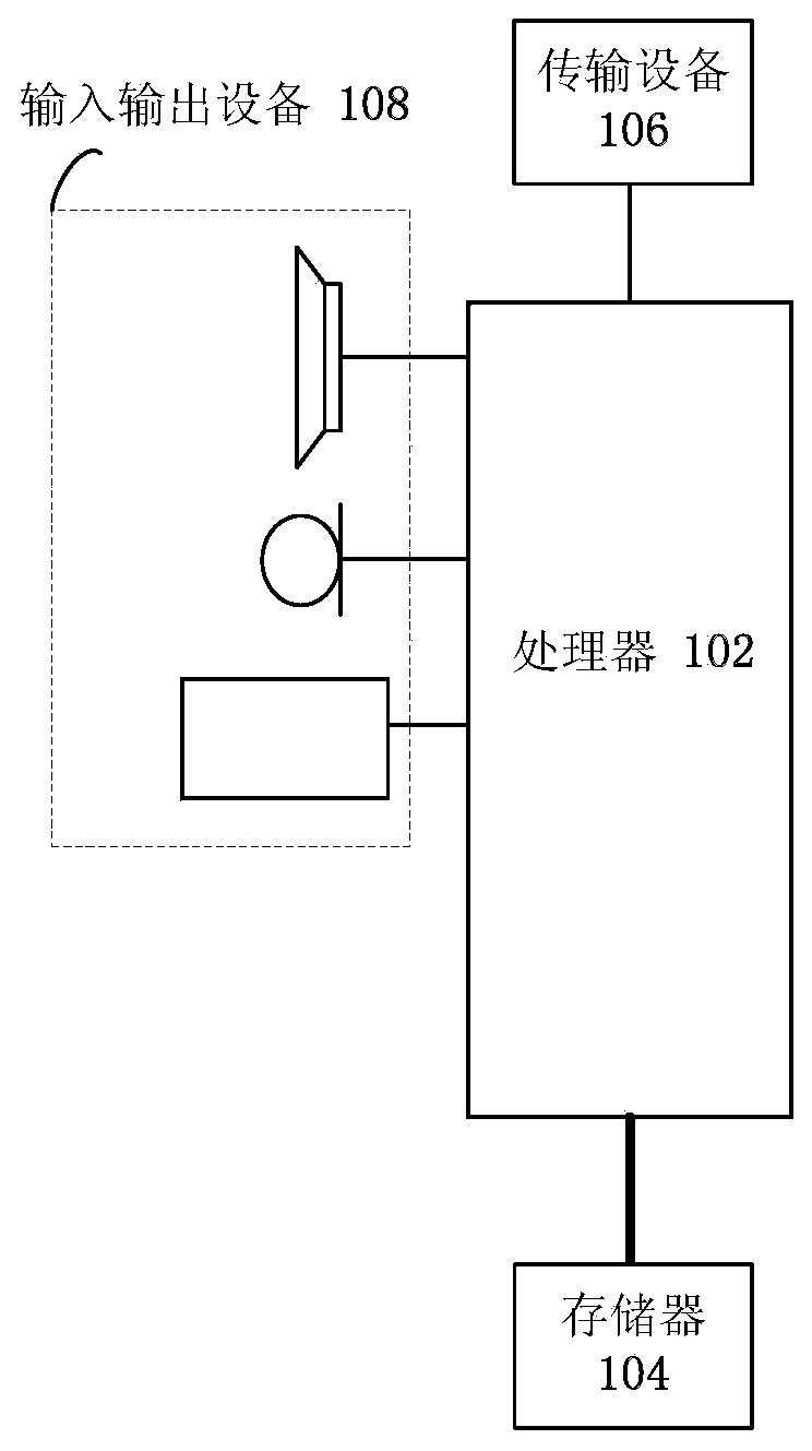
[0092] The method embodiment provided in Embodiment 1 of the present application may be executed in a mobile terminal, a computer terminal, or a similar computing device. Taking running on a mobile terminal as an example, figure 1 It is a block diagram of the hardware structure of a mobile terminal of a wafer positioning method according to an embodiment of the present invention, as figure 1 As shown, the mobile terminal 10 may include one or more ( figure 1 Only one is shown in the figure) a processor 102 (the processor 102 may include but not limited to a processing device such as a microprocessor MCU or a programmable logic device FPGA) and a memory 104 for storing data. Optionally, the above-mentioned mobile terminal also A transmission device 106 for communication functions as well as input and output devices 108 may be included. Those of ordinary skill in the art can understand that, figure 1 The shown structure is only for illustration, and does not limit the structu...

Embodiment 2

[0179] In this embodiment, a wafer positioning device is also provided, which is used to implement the above embodiments and preferred implementation modes, and what has been explained will not be repeated here. As used below, the term "module" may be a combination of software and / or hardware that realizes a predetermined function. Although the devices described in the following embodiments are preferably implemented in software, implementations in hardware, or a combination of software and hardware are also possible and contemplated.

[0180] Figure 10 is a block diagram of a wafer positioning device according to an embodiment of the present invention, such as Figure 10 shown, including:

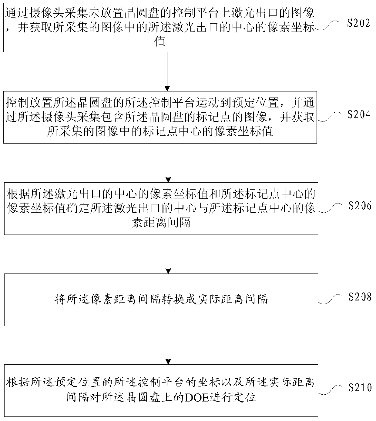
[0181] The first acquisition module 102 is configured to acquire an image of the laser outlet on the control platform where no wafer is placed through the camera, and acquire the pixel coordinate value of the center of the laser outlet in the collected image;

[0182] The second acquis...

Embodiment 3

[0216] An embodiment of the present invention also provides a storage medium, in which a computer program is stored, wherein the computer program is set to execute the steps in any one of the above method embodiments when running.

[0217] Optionally, in this embodiment, the above-mentioned storage medium may be configured to store a computer program for performing the following steps:

[0218] S11, collecting an image of the laser outlet on the control platform where the wafer is not placed through the camera, and obtaining the pixel coordinate value of the center of the laser outlet in the collected image;

[0219] S12, controlling the control platform on which the wafer is placed to move to a predetermined position, and collecting an image including a marking point of the wafer through the camera, and acquiring a pixel at the center of the marking point in the collected image coordinate value;

[0220] S13. Determine the pixel distance interval between the center of the la...


PUM


Abstract

The invention provides a wafer disc positioning method and device, wherein the method comprises the steps of collecting an image of a laser outlet in a control platform where a wafer disc is not placed through a camera, and obtaining a pixel coordinate value of the center of the laser outlet; controlling the control platform on which the wafer disc is placed to move to a preset position, collecting an image containing a mark point of the wafer disc through a camera, and obtaining a pixel coordinate value of the center of the mark point; determining a pixel distance interval between the centerof the laser outlet and the center of the mark point according to the pixel coordinate value of the center of the laser outlet and the pixel coordinate value of the center of the mark point; converting the pixel distance interval into an actual distance interval; and positioning the wafer disc according to the coordinates of the control platform at the predetermined position and the actual distance interval, so that the problem of how to realize high-precision fine positioning of the wafer disc through machine vision in the prior art can be solved, and the effect of high-precision fine positioning of the wafer disc is realized.

Description

technical field [0001] The present invention relates to the communication field, in particular, to a wafer positioning method and device. Background technique [0002] With the development of computer vision technology, more and more applications can play a role in industrial inspection. In the solution for testing DOE performance, the size of the laser spot is very close to the size of the DOE’s appearance, and the position of the laser spot is offset from the DOE, which will cause light leakage and cause the center of the DOE diffraction spot to be too bright, which may cause false detection. Therefore, the precise coordinate positioning of DOE is very important for DOE performance testing. [0003] When testing all the DOEs of the wafer disk, there are thousands of DOEs in total. If manual positioning is used, the workload is huge and it is not suitable for fast and large-scale test scenarios. Therefore, in order to meet the DOE coordinates of the wafer disk High-precis...

Claims


Application Information

Patent Timeline
IPC IPC(8): G06T7/00G06T7/62G06T7/73
Inventor 赵晓琛
Owner ZHEJIANG SUNNY OPTICAL CO LTD
Why Eureka
Try Eureka