Display panel and manufacturing method thereof

A display panel and substrate substrate technology, applied in optics, instruments, electrical components, etc., can solve problems affecting circuit reliability and stability, threshold voltage drift, affecting stability, etc., to avoid adverse effects and stabilize the threshold The effect of voltage

Inactive Publication Date: 2019-06-14
TCL CHINA STAR OPTOELECTRONICS TECH CO LTD
View PDF8 Cites 0 Cited by
  • Summary
  • Abstract
  • Description
  • Claims
  • Application Information

AI Technical Summary

Problems solved by technology

However, the threshold voltage drift of the oxide thin film transistor will occur after a long time of operation, which seriously affects the reliability and stability of the circuit with the thin film transistor as the device. One of the important reasons for the threshold voltage drift of the thin film transistor is air Water vapor enters the interface of metal oxide and other film layers through the film, affecting the stability

Method used


Image

  • Display panel and manufacturing method thereof
  • Display panel and manufacturing method thereof
  • Display panel and manufacturing method thereof

Examples


Embodiment Construction

[0021] The following descriptions of the various embodiments refer to the accompanying drawings to illustrate specific embodiments in which the present invention can be practiced. The directional terms mentioned in the present invention, such as "up", "down", "front", "back", "left", "right", "inside", "outside", "side", etc., are for reference only The orientation of the attached schema. Therefore, the directional terms used are used to illustrate and understand the present invention, but not to limit the present invention.

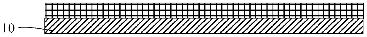
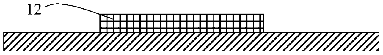
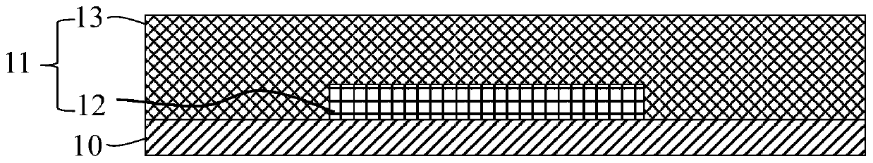
[0022] The present invention is a display panel, which can be a liquid crystal display panel or an organic light emitting display panel. Figures 1A-1H Each is a schematic cross-sectional view of a partial structure of a display panel according to a preferred embodiment of the present invention, wherein each schematic cross-sectional view of a partial structure can also be used as a description of the process for manufacturing the display panel of the p...


PUM


Abstract

The invention discloses a display panel. The display panel comprises a substrate, an active layer, a structural layer, a passivation layer and a pixel definition layer. The active layer is arranged onthe substrate. The structural layer is arranged on the active layer and comprises an oxide semiconductor layer. The passivation layer is arranged on the structural layer and comprises an inorganic material layer and a titanium dioxide layer. The pixel definition layer is arranged on the passivation layer. A hydrophobic membrane structure is formed by the titanium dioxide layer under the catalysisof ultraviolet light.

Description

【Technical field】 [0001] The invention relates to the field of display technology, in particular to a display panel and a manufacturing method thereof. 【Background technique】 [0002] The thin-film transistor (thin-film transistor, TFT) array substrate is the main component in the current liquid crystal display device and active matrix organic light emitting diode (active matrix organic light emitting diode, AMOLED) display device, and is used to provide the drive for the display. circuit. The array substrate is usually provided with several gate scanning lines and several data lines, which together define a plurality of pixel units. Each pixel unit is provided with a thin film transistor and a pixel electrode. The gate of the thin film transistor is connected to the corresponding gate scanning line. When the voltage on the gate scanning line reaches the turn-on voltage, the source and drain of the thin film transistor are turned on. , so that the data voltage on the data ...

Claims


Application Information

Patent Timeline
Patent Type & Authority Applications(China)
IPC IPC(8): H01L27/12H01L27/32G02F1/1368
Inventor 林钦遵
Owner TCL CHINA STAR OPTOELECTRONICS TECH CO LTD
Why Eureka
Try Eureka