

String select line gate oxide method for 3D vertical channel NAND memory
- Summary
- Abstract
- Description
- Claims
- Application Information
AI Technical Summary
Benefits of technology
Problems solved by technology
Method used
Image

Examples
Embodiment Construction
[0020]A detailed description of embodiments of the present invention is provided with reference to the FIGS. 1-30. The following description will typically be with reference to specific structural embodiments and methods. It is to be understood that there is no intention to limit the invention to the specifically disclosed embodiments and methods but that the invention may be practiced using other features, elements, methods, and embodiments. Preferred embodiments are described to illustrate the present invention, not to limit its scope, which is defined by the claims. Those of ordinary skill in the art will recognize a variety of equivalent variations on the description that follows.
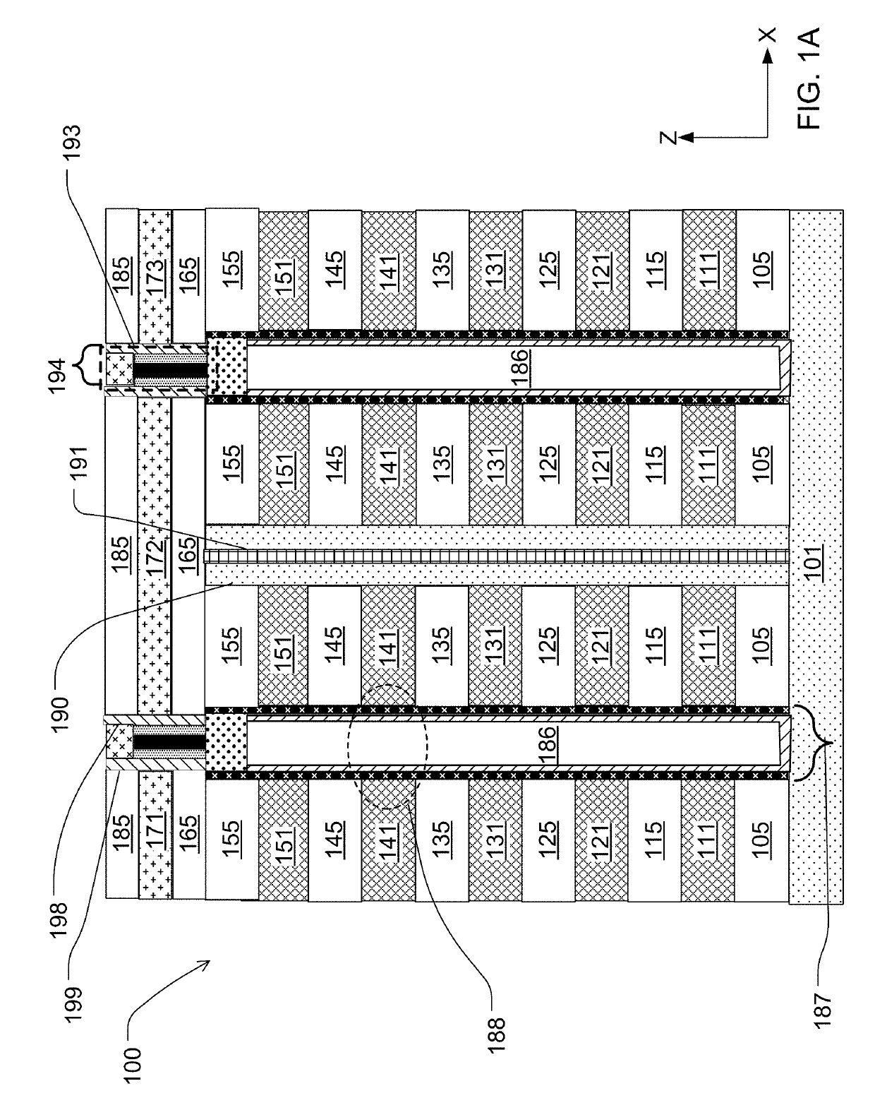
[0021]FIG. 1A is a cross-sectional diagram of a 3D memory device 100 according to an embodiment of the present invention, shown in an X-Z plane. As illustrated in the example of FIG. 1A, a memory device 100 includes an array of NAND strings of memory cells formed over a conductive well in substrate 101....
PUM
 Abstract
Description
Claims
Application Information