Method for enabling SONOS (Silicon Oxide Nitride Oxide Semiconductor) transistor to double as switch and memory

A transistor and memory technology, applied in the field of maintaining a stable critical voltage, can solve the problems of large energy consumption, lower reliability, deterioration, etc., and achieve the effect of high memory density

Active Publication Date: 2011-05-11
ACER INC
View PDF8 Cites 2 Cited by
  • Summary
  • Abstract
  • Description
  • Claims
  • Application Information

AI Technical Summary

Problems solved by technology

The disadvantage is that channel thermal electron writing requires a lot of energy (power consumption). If multiple memory cells are written at the same time, power consumption is a big problem.
In addition, hot electron writing to the memory will cause degradation and reduce reliability.
The advantage of FN tunneling writing is that it does not need to consume a lot of power, but after FN tunneling, electrons will be injected into the silicon nitride layer above the entire channel, which cannot achieve a two-bit memory effect.

Method used


Image

  • Method for enabling SONOS (Silicon Oxide Nitride Oxide Semiconductor) transistor to double as switch and memory
  • Method for enabling SONOS (Silicon Oxide Nitride Oxide Semiconductor) transistor to double as switch and memory
  • Method for enabling SONOS (Silicon Oxide Nitride Oxide Semiconductor) transistor to double as switch and memory

Examples


Embodiment Construction

[0041] The following will refer to the relevant drawings to illustrate a method for making the SONOS transistor both a switch and a memory according to a preferred embodiment of the present invention. For ease of understanding, the same elements in the following embodiments are marked with the same symbols illustrate.

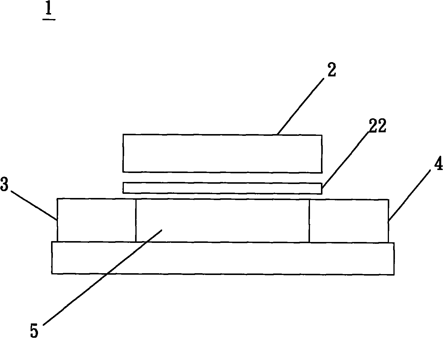
[0042] see figure 1 , figure 1 It is a schematic diagram of the non-volatile memory of the SONOS (Silicon-oxide-nitride-oxide-silicon) structure of the present invention. The transistor 1 includes a gate 2 , a charge storage layer 22 , a source 3 , a drain 4 and a substrate 5 . The transistor 1 can be a thin film transistor or a field effect transistor. Wherein the charge storage layer of the SONOS transistor is a silicon nitride layer, an aluminum oxide layer, a tantalum oxide layer or a titanium oxide layer

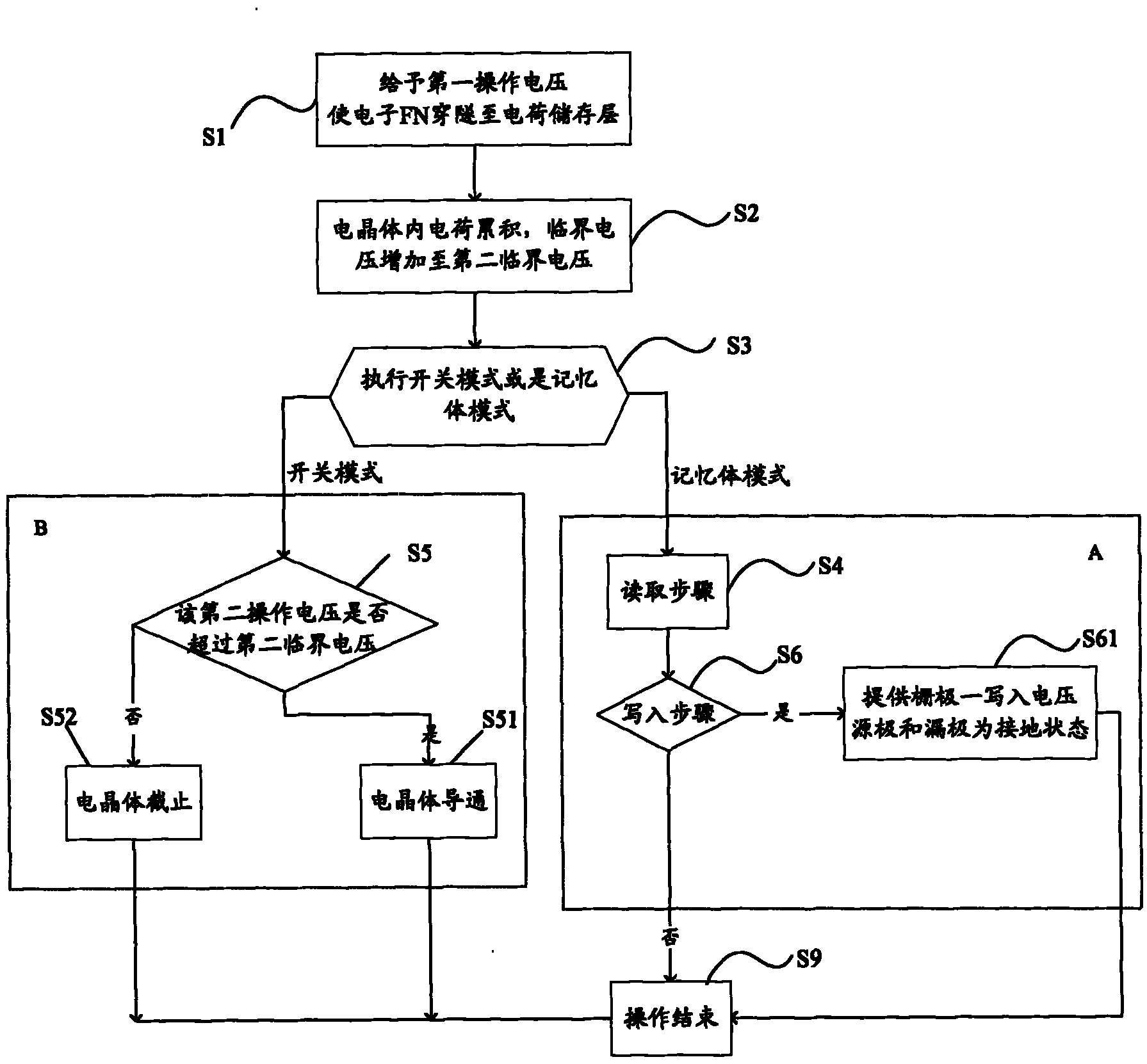
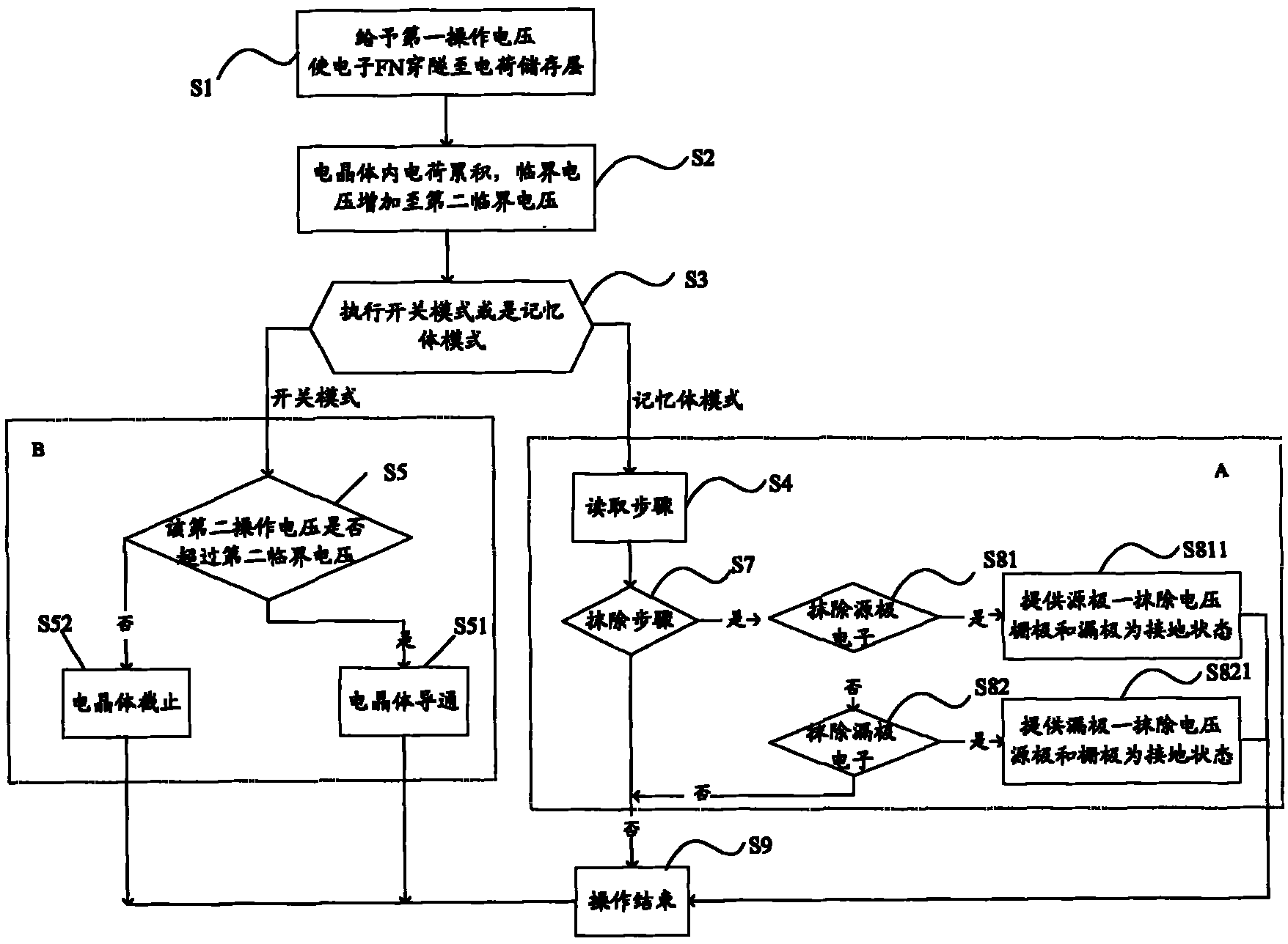
[0043] see figure 2 , figure 2It is an operation flowchart of another preferred embodiment of the present invention. The present invention oper...


PUM


Abstract

The invention discloses a method for enabling an SONOS (Silicon Oxide Nitride Oxide Semiconductor) transistor to double as a switch and a memory. The method comprises the following steps of: carrying out FN (Fowler-Nordheim) tunneling by utilizing a source electrode terminal or a drain electrode terminal of the memory; further changing an electronic storage state in an electric charge storage layer at the upside near the source electrode terminal or the drain electrode terminal; and judging a memory state of a drain electrode or a source electrode by utilizing grid induction drain leakage current change, wherein the transistor always maintains a stable critical voltage in the operation state. In the method, the single transistor is enabled to have dual characteristics of the switch and the memory simultaneously and have a binary memory effect, and a memory density higher than that of the common memory can be provided.

Description

technical field [0001] The present invention relates to a method for making the SONOS transistor both a switch and a memory, and in particular relates to a method capable of maintaining a stable critical voltage. Background technique [0002] At present, the general way of flash memory (flash type nonvolatile memory) to judge the memory state is to apply a threshold voltage (Threshold voltage) between the write (program) and erase (erase) threshold voltage on the gate (gate). Read the voltage Vread to read the corresponding current, so as to judge whether the memory state is "0" or "1". The size of the critical voltage difference (or memory window) between writing and erasing will affect the misjudgment probability of the memory state. The memory window must be large to avoid misjudgment of the memory state. Once the threshold voltage of the memory is changed, the transistor cannot be switched on and off correctly, so it cannot be used as a switch. [0003] There are two t...

Claims


Application Information

Patent Timeline
IPC IPC(8): G11C16/06G11C16/10G11C16/14H03K17/687
Inventor 张鼎张陈世青陈德智简富彦徐咏恩
Owner ACER INC
Why Eureka
Try Eureka