Graphene transparent conductive film, its preparation method, and liquid crystal film
A transparent conductive film, graphene technology, applied in instruments, nonlinear optics, optics, etc., can solve the problems of easy breakdown of the substrate, inability to meet the pre-tilt angle, foreign matter affecting the yield and quality of liquid crystal display devices, etc.
- Summary
- Abstract
- Description
- Claims
- Application Information
AI Technical Summary
Problems solved by technology
Method used
Image
Examples
Embodiment 1
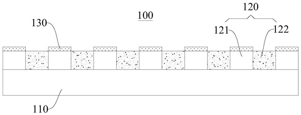
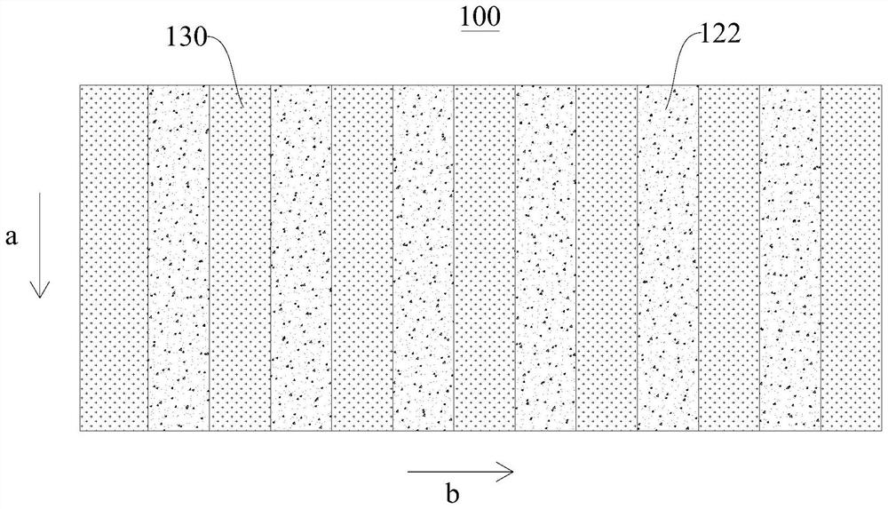
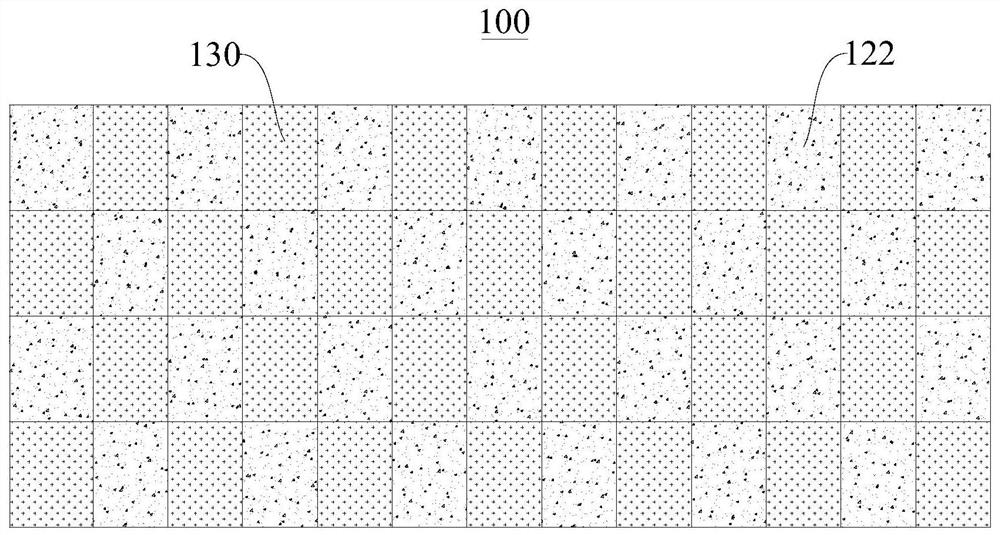
[0083] A graphene transparent conductive film 100 includes a substrate layer 110 , a patterned graphene layer 120 and a vertical alignment layer 130 arranged in sequence.
[0084] Wherein, the material of the substrate layer 110 is PI, and the thickness is 0.5 μm. The thickness of the patterned graphene layer 120 is 0.3 nm. The vertical alignment agent constituting the vertical alignment layer 130 is dodecylbenzenesulfonic acid. The area percentages of the vertical alignment layer 130 and the graphene region 122 are 5%:95%.
[0085] A preparation method of the above-mentioned graphene transparent conductive film 100, comprising:
[0086] The substrate layer 110 is ultrasonically cleaned with ethanol, acetone, and deionized water, rinsed with deionized water, and then air-dried or oven-dried with nitrogen.
[0087] A graphene layer is formed on the surface of the cleaned substrate layer 110 by chemical vapor deposition. The graphene layer is covered with a fine metal mask, ...
Embodiment 2
[0089] A graphene transparent conductive film 100 includes a substrate layer 110 , a patterned graphene layer 120 and a vertical alignment layer 130 arranged in sequence.
[0090] Wherein, the material of the substrate layer 110 is PET, and the thickness is 1 μm. The thickness of the patterned graphene layer 120 is 0.35 nm. The vertical alignment agent constituting the vertical alignment layer 130 is octadecylbenzenesulfonic acid. The area percentages of the vertical alignment layer 130 and the graphene region 122 are 30%:70%.
[0091] A preparation method of the above-mentioned graphene transparent conductive film 100, comprising:
[0092] The substrate layer 110 is ultrasonically cleaned with ethanol, acetone, and deionized water, rinsed with deionized water, and then air-dried or oven-dried with nitrogen.
[0093] A graphene oxide layer is formed on the surface of the cleaned substrate layer 110 by a spin coating method. The graphene oxide layer is covered with a fine m...
Embodiment 3
[0095] A graphene transparent conductive film 100 includes a substrate layer 110 , a patterned graphene layer 120 and a vertical alignment layer 130 arranged in sequence.
[0096] Wherein, the material of the substrate layer 110 is PI, and the thickness is 10 μm. The thickness of the patterned graphene layer 120 is 1.1 nm. The vertical alignment agent constituting the vertical alignment layer 130 is 1,4'-dodecyloxy-4-hydroxybiphenyl. The area percentages of the vertical alignment layer 130 and the graphene region 122 are 50%:50%.
[0097] A preparation method of the above-mentioned graphene transparent conductive film 100, comprising:
[0098] The substrate layer 110 is ultrasonically cleaned with ethanol, acetone, and deionized water, rinsed with deionized water, and then air-dried or oven-dried with nitrogen.
[0099] A graphene layer is formed on the surface of the cleaned substrate layer 110 by chemical vapor deposition. The graphene layer is covered with a fine metal ...
PUM
| Property | Measurement | Unit |
|---|---|---|
| thickness | aaaaa | aaaaa |
| thickness | aaaaa | aaaaa |
| thickness | aaaaa | aaaaa |
Abstract
Description
Claims
Application Information
 - R&D Engineer
- R&D Manager
- IP Professional
- Industry Leading Data Capabilities
- Powerful AI technology
- Patent DNA Extraction
Browse by: Latest US Patents, China's latest patents, Technical Efficacy Thesaurus, Application Domain, Technology Topic, Popular Technical Reports.
© 2024 PatSnap. All rights reserved.Legal|Privacy policy|Modern Slavery Act Transparency Statement|Sitemap|About US| Contact US: help@patsnap.com


