Stacked structure for parallel capacitors and method of fabrication

a technology of parallel capacitors and stacked structures, which is applied in the direction of resistors, basic electric elements, solid-state devices, etc., can solve the problems of limited physical size of capacitor networks, the reduction of the area requirements of passive devices, and the inability to keep up with the reduction of active device feature sizes

Inactive Publication Date: 2005-01-04
BELL SEMICON LLC +1
View PDF5 Cites 52 Cited by
  • Summary
  • Abstract
  • Description
  • Claims
  • Application Information

AI Technical Summary

Problems solved by technology

However, in many instances, reductions in the area requirements for passive devices have not kept pace with reduced feature sizes of active devices and metallization.
The physical size of a capacitor network is limited by several factors, including the required area of the capacitor plates as well as the thickness of the intervening dielectric.

Method used


Image

  • Stacked structure for parallel capacitors and method of fabrication
  • Stacked structure for parallel capacitors and method of fabrication
  • Stacked structure for parallel capacitors and method of fabrication

Examples


Embodiment Construction

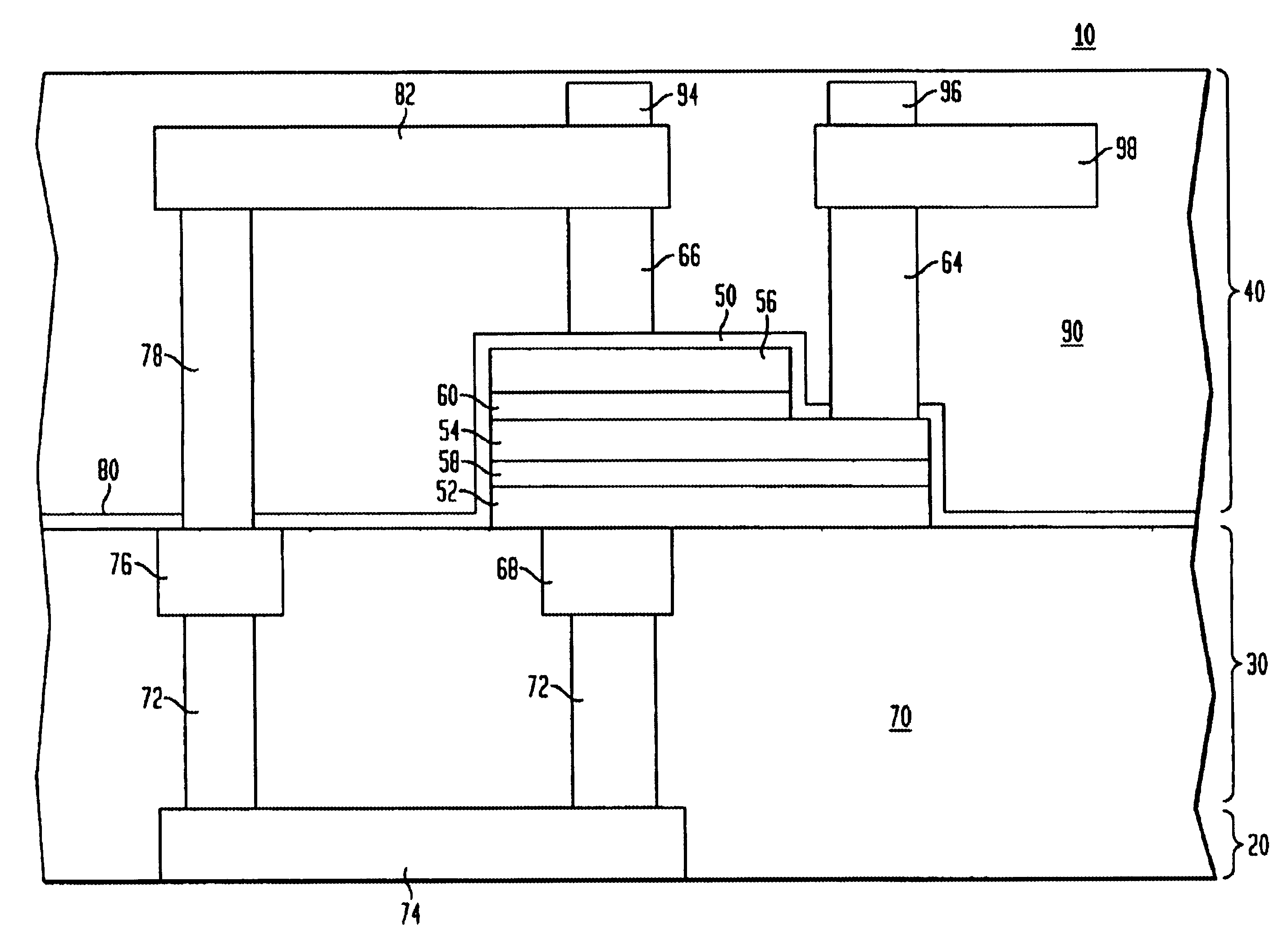
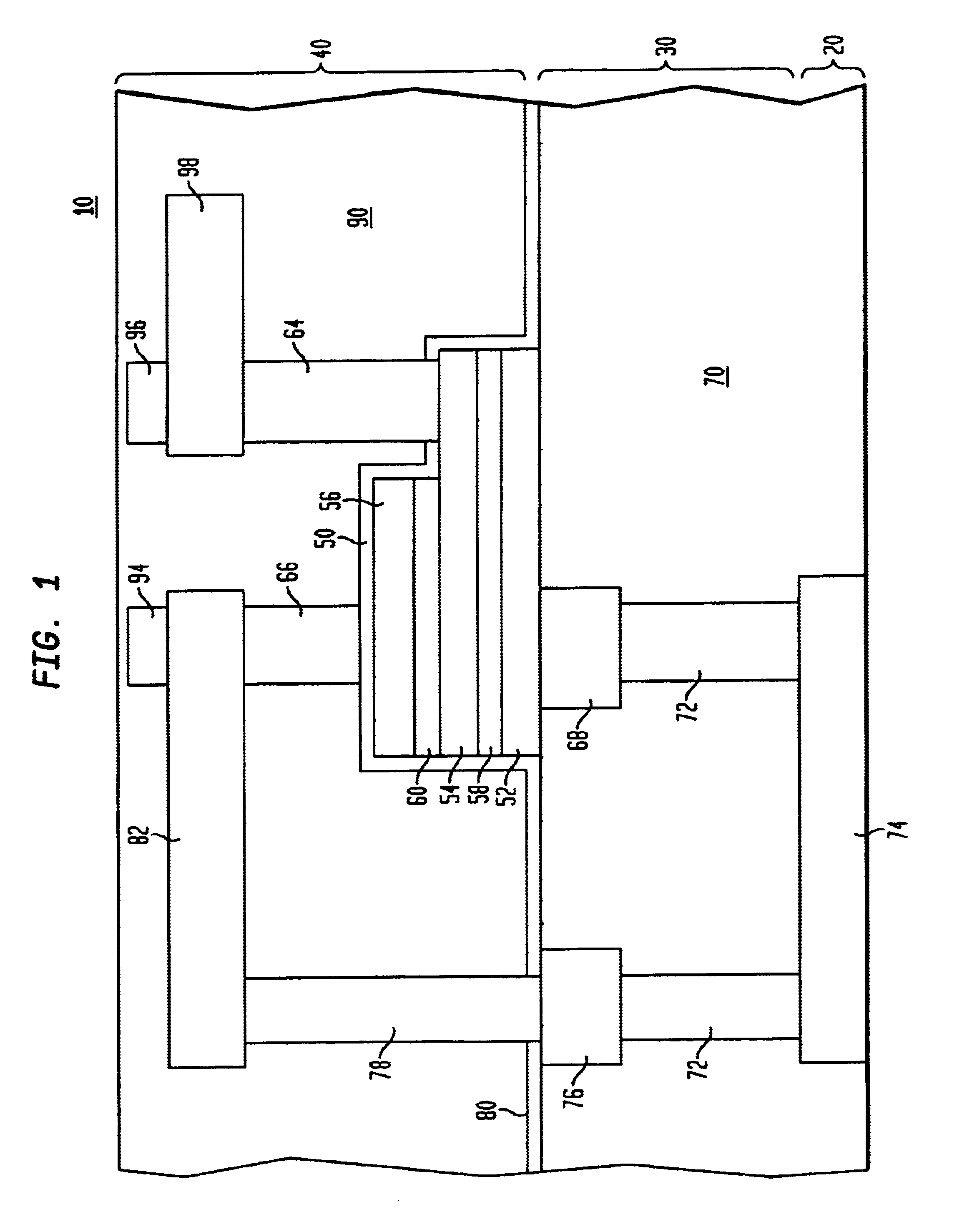
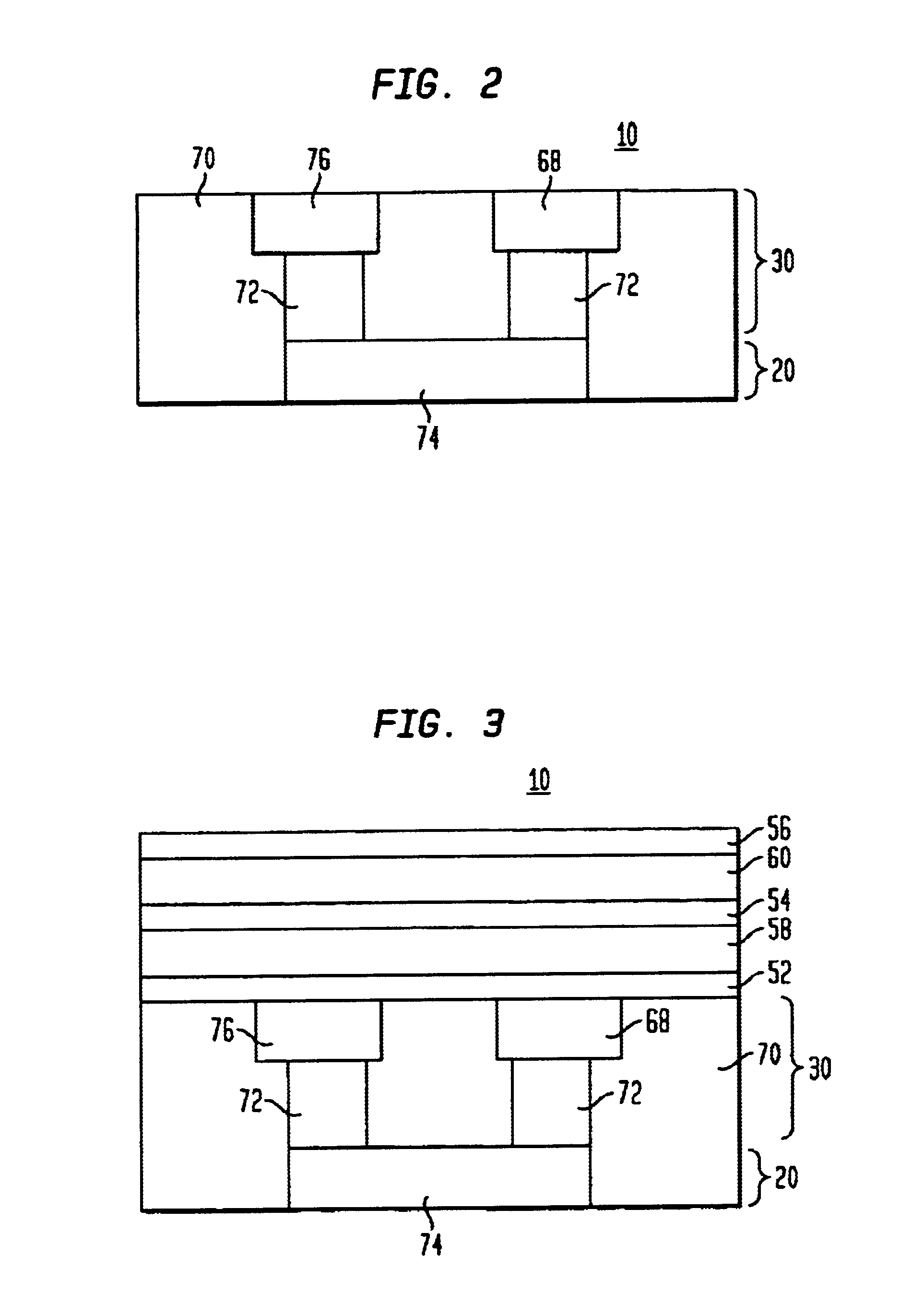
With reference to the view of FIG. 1, the invention is described with respect to formation and connection of an exemplary capacitor structure formed in three levels of interconnect metallization. A portion of an integrated circuit structure 10 is shown in partial cross section to provide details of the invention in a metallization structure. The metallization structure is formed over a semiconductor layer (not illustrated) which typically will have a plurality of transistors in the surface thereof. In this exemplary embodiment, several upper levels of metal interconnect, such as Al or Cu runners, are formed over the semiconductor layer according to a dual Damascene fabrication process. Specifically, a portion of the integrated circuit structure 10 is shown in FIG. 1 to include three sequentially formed levels of metallization 20, 30 and 40. One or more additional levels of metallization may be formed below level 20 and one or more additional levels of metallization may be formed abo...


PUM


Abstract

A monolithic integrated circuit including a capacitor structure. In one embodiment the integrated circuit includes at least first and second levels of interconnect conductor for connection to a semiconductor layer and a stack of alternating conductive and insulative layers formed in vertical alignment with respect to an underlying plane. The stack is formed between the first and second levels of conductor. Preferably the stack includes a first conductive layer, a first insulator layer formed over the first conductive layer, a second conductive layer formed over the first insulative layer, a second insulator layer formed over the second conductive layer, and a third conductive layer formed over the second insulative layer, with the first and third conductive layers commonly connected.

Description

FIELD OF THE INVENTIONThe present invention relates to semiconductor devices and, more specifically, to devices having capacitor structures formed in metallization levels over a semiconductor layer.BACKGROUND OF THE INVENTIONAs the level of semiconductor process integration has progressed, advances in the technology have been largely focused on reducing feature sizes and layout geometry of active devices as well as increasing the density of metallization. However, in many instances, reductions in the area requirements for passive devices have not kept pace with reduced feature sizes of active devices and metallization. For example, the layout area required for resistors is largely determined by the sheet resistance. The physical size of a capacitor network is limited by several factors, including the required area of the capacitor plates as well as the thickness of the intervening dielectric. That is, as dielectric thickness decreases the capacitance increases such that the capacito...

Claims


Application Information

Patent Timeline
Patent Type & Authority Patents(United States)
IPC IPC(8): H01L23/522H01L21/02H01L23/52H01L21/3205H01L21/768H01L21/822H01L27/04
CPCH01L23/5223H01L28/40H01L2924/0002H01L2924/00H01L27/04
Inventor YEN, ALLENHUI, FRANK YAUCHEEYAN, YIFENG WINSTON
Owner BELL SEMICON LLC
Why Eureka
Try Eureka