Conductor treating single-wafer type treating device and method for semi-conductor treating

a technology of treating device and semiconductor, which is applied in the direction of chemistry apparatus and processes, crystal growth processes, coatings, etc., can solve the problems of defective or lower electrical characteristics of semiconductor devices

Inactive Publication Date: 2007-06-26
TOKYO ELECTRON LTD
View PDF12 Cites 577 Cited by
  • Summary
  • Abstract
  • Description
  • Claims
  • Application Information

AI Technical Summary

Benefits of technology

[0014]performing a second process while supplying the heating medium into the flow passage to se

Problems solved by technology

The natural oxide film can cause the semiconductor devices

Method used


Image

  • Conductor treating single-wafer type treating device and method for semi-conductor treating
  • Conductor treating single-wafer type treating device and method for semi-conductor treating
  • Conductor treating single-wafer type treating device and method for semi-conductor treating

Examples


Embodiment Construction

[0033]In the process of developing the present invention, the inventors studied the case of performing the pre-cleaning method disclosed in Jpn. Pat. Appln. KOKAI Publication No. 2-256235, while assuming an apparatus model for converting an oxide film into an intermediate, and an apparatus model for sublimating the intermediate. FIGS. 10 and 11 are constitutional views respectively showing an apparatus model for forming an intermediate and an apparatus model for sublimating the intermediate.

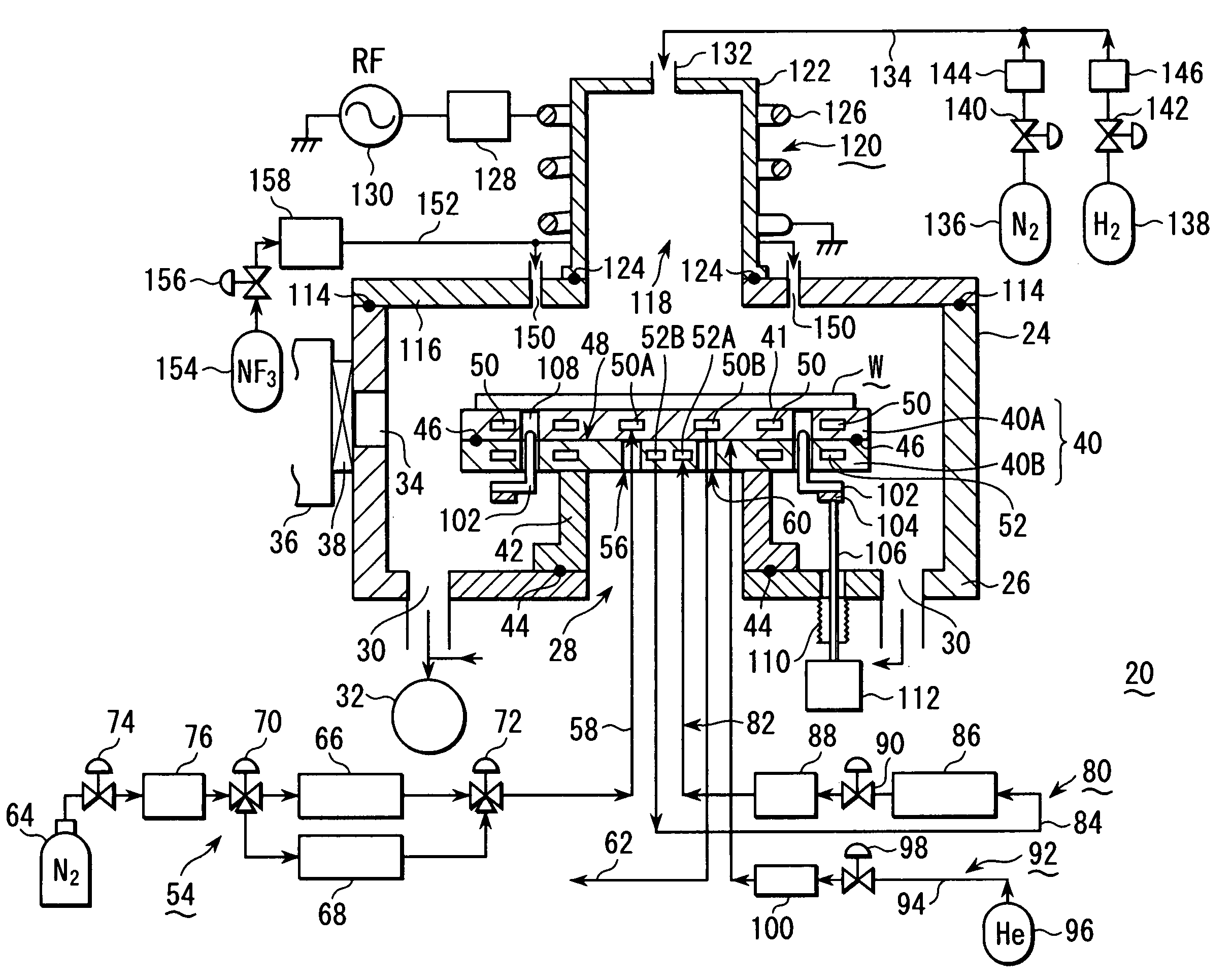
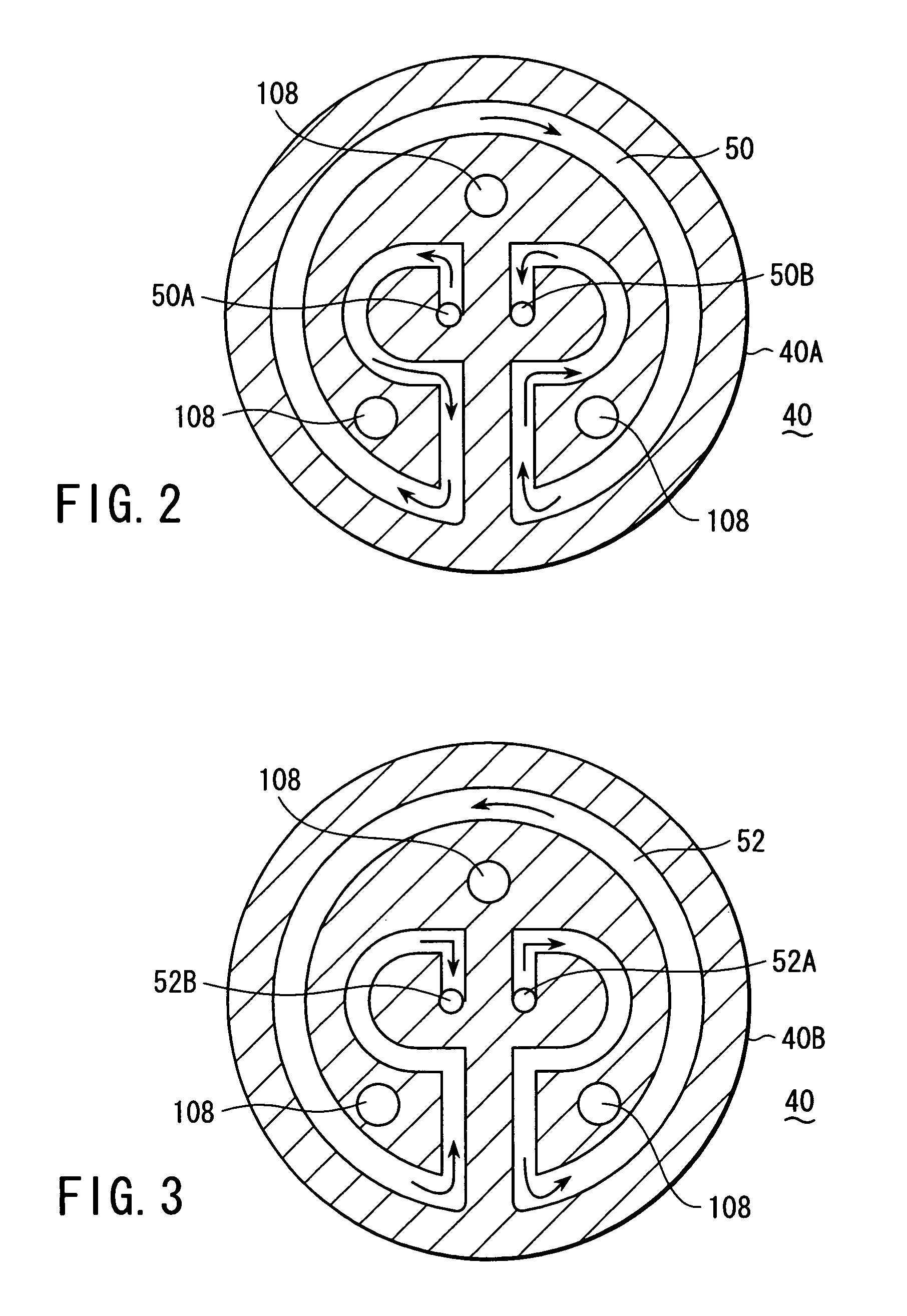
[0034]As shown in FIG. 10, the processing apparatus 1 has a process chamber 2, which can be vacuum-exhausted, and a worktable 4, on which a semiconductor wafer W formed of a silicon wafer is placed. An unnecessary natural oxide film has already been formed on the surface of the wafer W. On the ceiling of the process chamber 2, a remote plasma generating mechanism 6 is disposed, for forming plasma from N2 gas and H2 gas by a radio frequency (RF) power of 13.56 MHz. The plasma is utilized to genera...


PUM

PropertyMeasurementUnit
Temperatureaaaaaaaaaa

Abstract

A single-substrate processing apparatus (20) has a worktable (40) disposed in a process chamber (24), which accommodates a target substrate (W). The worktable (40) has a thermally conductive mount surface (41) to place the target substrate (W) thereon. The worktable (40) is provided with a flow passage (50) formed therein, in which a thermal medium flows for adjusting temperature of the target substrate (W) through the mount surface (41). The flow passage (50) is connected to a thermal medium supply system (54), which selectively supplies a cooling medium and a heating medium.

Description

TECHNICAL FIELD[0001]The present invention relates to a single-substrate processing apparatus and method for a semiconductor process, which performs a process such as oxide film removal, annealing, film formation, etching, oxidation, or diffusion. The term “semiconductor process” used herein includes various kinds of processes which are performed to manufacture a semiconductor device or a structure having wiring layers, electrodes, and the like to be connected to a semiconductor device, on a target substrate, such as a semiconductor wafer or an LCD substrate, by forming semiconductor layers, insulating layers, and conductive layers in predetermined patterns on the target substrate.BACKGROUND ART[0002]In the process of manufacturing semiconductor devices, a semiconductor wafer is subjected to processes of various kinds, such as film-formation, oxidation, diffusion, annealing, reformation, and etching. Before the processes, there may be a natural oxide film (consisting of SiO2 if the ...

Claims


Application Information

Patent Timeline
IPC IPC(8): H01L21/302C23C16/00B44C1/22C23C16/46C03C15/00C23C16/511C23F1/00C30B31/14C30B31/16H01L21/00H01L21/28H01L21/306H01L21/3065H01L21/324H01L21/768
CPCC30B31/14C30B31/16H01L21/67109H01L21/3065
Inventor KITAYAMA, HIROFUMIMATSUSHIMA, NORIAKI
Owner TOKYO ELECTRON LTD
Why Eureka
Try Eureka