Method of manufacturing semiconductor device having dual fully-silicided gate

a semiconductor device and fully-silicided technology, applied in the direction of semiconductor devices, basic electric elements, electrical appliances, etc., can solve the problems of device threshold voltage (vt) drop, reduced channel length, limited channel size of mos transistor, etc., to reduce manufacturing costs and simplify the process

Inactive Publication Date: 2011-12-01
UNITED MICROELECTRONICS CORP
View PDF13 Cites 8 Cited by
  • Summary
  • Abstract
  • Description
  • Claims
  • Application Information

AI Technical Summary

Benefits of technology

[0009]An objective of the present invention is to provide a method of manufacturing a semiconductor device having a dual fully-silicided gate, which can be used to fabricate two kinds of metal gates having different characteristics in one silicidation process, thereby simplifying the process and reducing the manufacturing cost.
[0035]According to an embodiment of the present invention, only one silicidation process is required to form the first silicided gate and the second silicided gate having different properties, thus an additional lithographic etching process is not required, and the process is simplified.
[0036]Moreover, the material layer is used to protect the first source / drain and the second source / drain, so when performing the silicidation process to form the first silicided gate and the second silicided gate simultaneously, the first metal layer is prevented from being further reacted with silicon in the first source / drain and the second source / drain.
[0063]According to an embodiment of the present invention, the materials of the first gate and the second gate are different. After removing the first cap layer and the second cap layer to expose the first gate and the second gate, a silicidation process is performed to form the first silicided gate and the second silicided gate having different properties. The additional lithographic etching process is not required, thus simplifying the process. Moreover, if the etching process instead of CMP is used to remove the first cap layer and the second cap layer, the process can also be simplified, and the cost can be reduced.
[0064]Moreover, the process temperature of the source / drain silicided layer is higher than that of the first silicided gate and the second silicided gate, and when forming the first silicided gate and the second silicided gate, the second metal layer is prevented from further reacting with the first source / drain and the second source / drain, thereby avoid influencing the device characteristics.

Problems solved by technology

However, the reduction of the channel size of the MOS transistor is limited.
When the length is reduced to a certain extent, various problems resulting from the reduction in the channel length occur, namely short channel effect.
The so-called short channel effect may cause a device threshold voltage (Vt) drop and poor control of the gate voltage (Vg) to the MOS transistor, and a punch-through effect also influences the operation of the MOS transistor.
Particularly, when the size of the MOS transistor is reduced to the nanometer scale, the short channel effect and the punch-through effect become serious, such that the semiconductor device cannot be further reduced.
However, the reduction in the thickness of the gate oxide layer incurs more serious polysilicon depletion, resulting in the reduction in the gate capacitance and decrease in the driving force.
In another aspect, when a high-K material is employed serving as the gate dielectric layer, Fermi level pinning issue occurs when the polysilicon gate contacts the high-K material, thus easily causing a higher threshold voltage (Vt) then reduce the device operation current.
Therefore, the process is quite complicated, and the manufacturing cost cannot be reduced.

Method used


Image

  • Method of manufacturing semiconductor device having dual fully-silicided gate
  • Method of manufacturing semiconductor device having dual fully-silicided gate
  • Method of manufacturing semiconductor device having dual fully-silicided gate

Examples


first embodiment

The First Embodiment

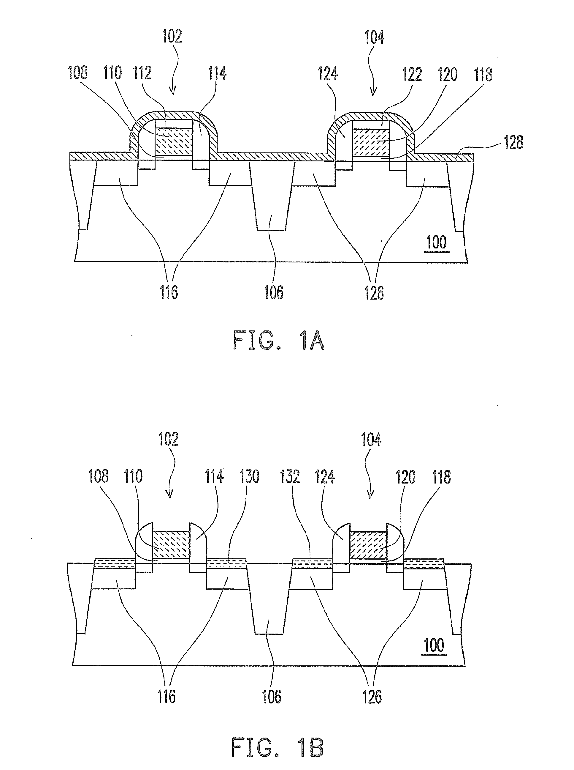
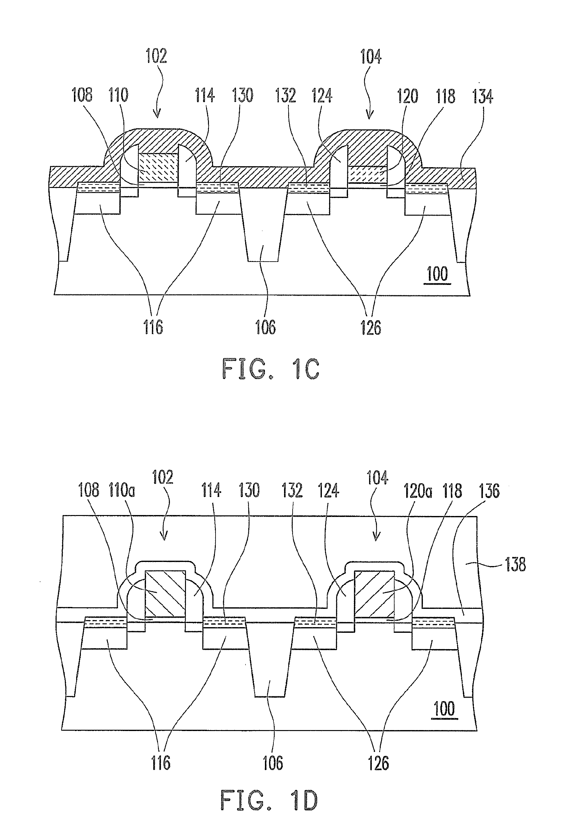
[0070]FIG. 1A to FIG. 1D are cross-sectional views of the process steps of the method of manufacturing the semiconductor device having a dual fully-silicided gate according to the first embodiment of the present invention.

[0071]Referring to FIG. 1A, first a substrate 100 is provided. The substrate 100 includes a silicon substrate, for example, an N-type silicon substrate or a P-type silicon substrate. The substrate 100 can be a silicon-on-insulating layer substrate and the like.

[0072]A transistor 102 and a transistor 104 are already formed on the substrate 100. The transistor 102 and the transistor 104 are isolated by, for example, device isolation structures 106. The device isolation structure 106 is, for example, a shallow trench isolation structure or a field oxide layer.

[0073]The transistor 102 includes, for example, a gate dielectric layer 108, a gate 110, a cap layer 112, spacers 114, and source / drain 116.

[0074]The gate dielectric layer 108 is disposed betw...

second embodiment

The Second Embodiment

[0101]FIG. 2A to FIG. 2D are cross-sectional views of the process steps of the method of manufacturing the semiconductor device having a dual fully-silicided gate according to the second embodiment of the present invention. The second embodiment is a modified process of the first embodiment, and in the second embodiment, the components same as those in the first embodiment are indicated with the same symbols, and the details thereof will not be described herein again.

[0102]Referring to FIG. 2A, first a substrate 100 is provided. The substrate 100 includes silicon substrate. A transistor 102 and a transistor 104 are already formed on the substrate 100. The transistor 102 and the transistor 104 are isolated by, for example, device isolation structures 106. The transistor 102 includes, for example, a gate dielectric layer 108, a gate 110, a cap layer 112, spacers 114, and source / drain 116. The transistor 104 includes, for example, a gate dielectric layer 118, a gat...

third embodiment

The Third Embodiment

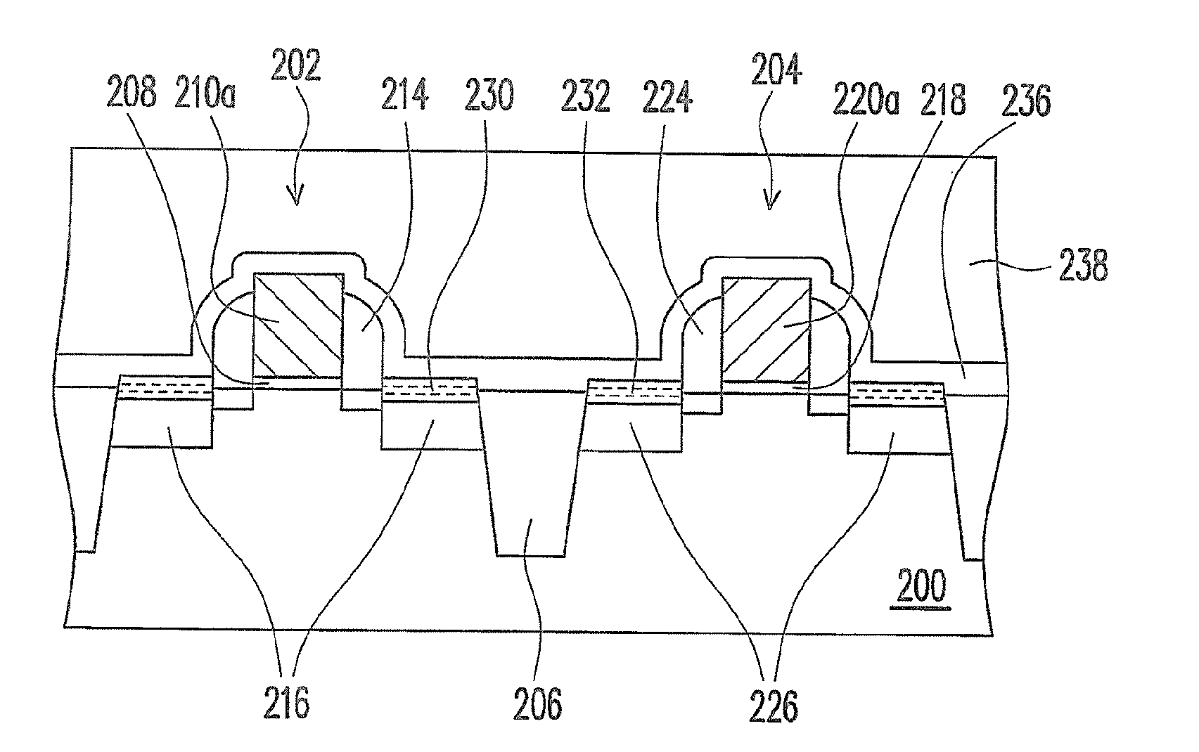
[0113]FIG. 3A to FIG. 3D are cross-sectional views of the process steps of the method of manufacturing the semiconductor device having a dual fully-silicided gate according to the third embodiment of the present invention.

[0114]Referring to FIG. 3A, first a substrate 200 is provided. The substrate 200 includes silicon substrate, for example, N-type silicon substrate or P-type silicon substrate. The substrate 200 can also be a silicon-on-insulating layer substrate and the like.

[0115]A transistor 202 and a transistor 204 are already formed on the substrate 200. The transistor 202 and the transistor 204 are isolated by, for example, device isolation structures 206. The device isolation structure 206 is, for example, a shallow trench isolation structure or a field oxide layer.

[0116]The transistor 202 includes, for example, a gate dielectric layer 208, a gate 210, spacers 214, and source / drain 216. The transistor 204 includes, for example, a gate dielectric layer 218,...


PUM


Abstract

A method of manufacturing the semiconductor device having a dual fully-silicided gate includes the following steps. A substrate having a first transistor and a second transistor formed thereon is provided, wherein the first transistor includes a first gate and a first source / drain and the second transistor includes a second gate and a second source / drain. The gate height of the first gate is different from that of the second gate. A first silicidation process is performed to respectively transform the first gate and the second gate into a first silicided gate and a second silicided gate simultaneously, wherein the material of the first silicided gate is different from that of the second silicided gate.

Description

CROSS-REFERENCE TO RELATED APPLICATION[0001]This application is a divisional application of and claims the priority benefit of U.S. application Ser. No. 11 / 620,984, filed on Jan. 8, 2007, now pending. The entirety of the above-mentioned patent application is hereby incorporated by reference herein and made a part of this specification.BACKGROUND OF THE INVENTION[0002]1. Field of the Invention[0003]The present invention relates to a method of manufacturing a semiconductor device. More particularly, the present invention relates to a method of manufacturing a semiconductor device having a dual fully-silicided gate.[0004]2. Description of Related Art[0005]With the increasing integration of integrated circuits, the dimension of semiconductor devices is gradually reduced accordingly. As the dimension of the metal oxide semiconductor (MOS) transistor is reduced, the channel length thereof must be reduced as well. However, the reduction of the channel size of the MOS transistor is limited....

Claims


Application Information

Patent Timeline
Patent Type & Authority Applications(United States)
IPC IPC(8): H01L21/263
CPCH01L21/28097H01L21/823835H01L29/66545H01L29/517H01L29/665H01L29/4975
Inventor LIN, CHIN-HSIANGHSU, CHIA-JUNGCHENG, LI-WEIMENG, HSIEN-LIANGWEI, MING-TEHSU, CHE-HUA
Owner UNITED MICROELECTRONICS CORP
Why Eureka
Try Eureka