Light Source With Glass Housing

a glass housing and light source technology, applied in the field of light sources, can solve the problems of light extraction, reduced efficiency with which light may be extracted from the device, and large heat dissipation of light emitting devices

Inactive Publication Date: 2008-08-28
KONINKLIJKE PHILIPS ELECTRONICS NV
View PDF5 Cites 8 Cited by
  • Summary
  • Abstract
  • Description
  • Claims
  • Application Information

AI Technical Summary

Benefits of technology

[0011]It is an object of the present invention to at least partly overcome the problems with the prior art, and to provide a LED-based light source that is temperature stable wherein steps in the manufacturing may involve temperatures higher than the break down temperature of the LEDs. Thus, in a first aspect, the present invention relates to a light source comprising at least one light-emitting diode, which emits light, and a housing arranged to receive at least a portion of said light. The housing comprises a translucent glass material and is provided with at least one recess that comprises positioning and orientating means. In the light source, the at least one light-emitting diode is arranged in the at least one recess, is positioned and orientated by the positioning and orientating means and is bonded to the housing.

Problems solved by technology

Light extraction is a key issue for light emitting devices.
A common problem of semiconductor light-emitting devices is that the efficiency with which light may be extracted from the device is reduced due to internal reflection in the interface between the device and the surroundings, followed by re-absorption of the reflected light in the device.
However, in high power applications, where single solid-state light emitting devices with an effect of up to 3 Watts per square mm or arrays of such devices, with a total effect of up to 100 Watts or more, a lot of heat is dissipated from the light emitting devices.
However, the processing temperature for connecting the coating material and the light emitting element must be low, e.g. lower than ˜350° C., or otherwise, the n / p-junctions in the light emitting element will be damaged.
However, substrates and circuitry on which light-emitting semiconductor devices are arranged are often heat sensitive.

Method used


Image

  • Light Source With Glass Housing
  • Light Source With Glass Housing
  • Light Source With Glass Housing

Examples


Embodiment Construction

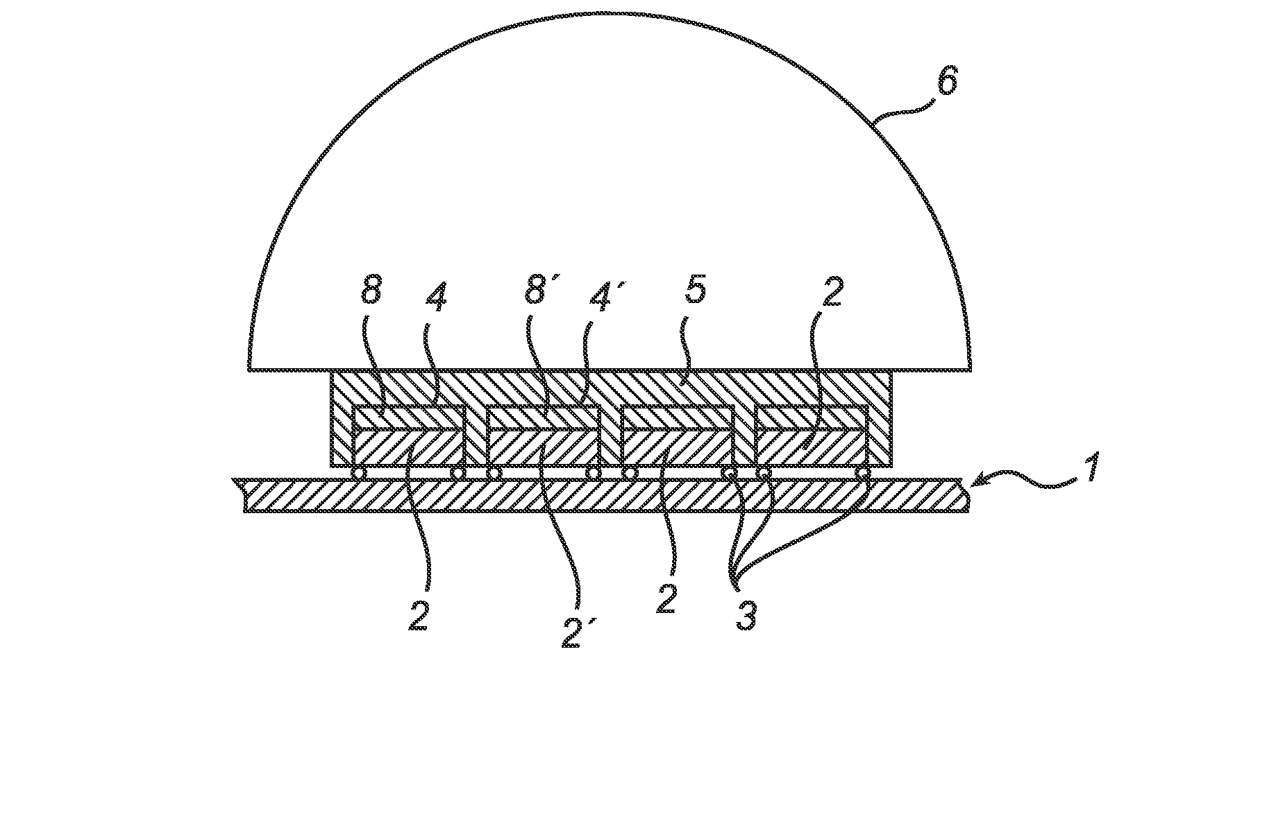
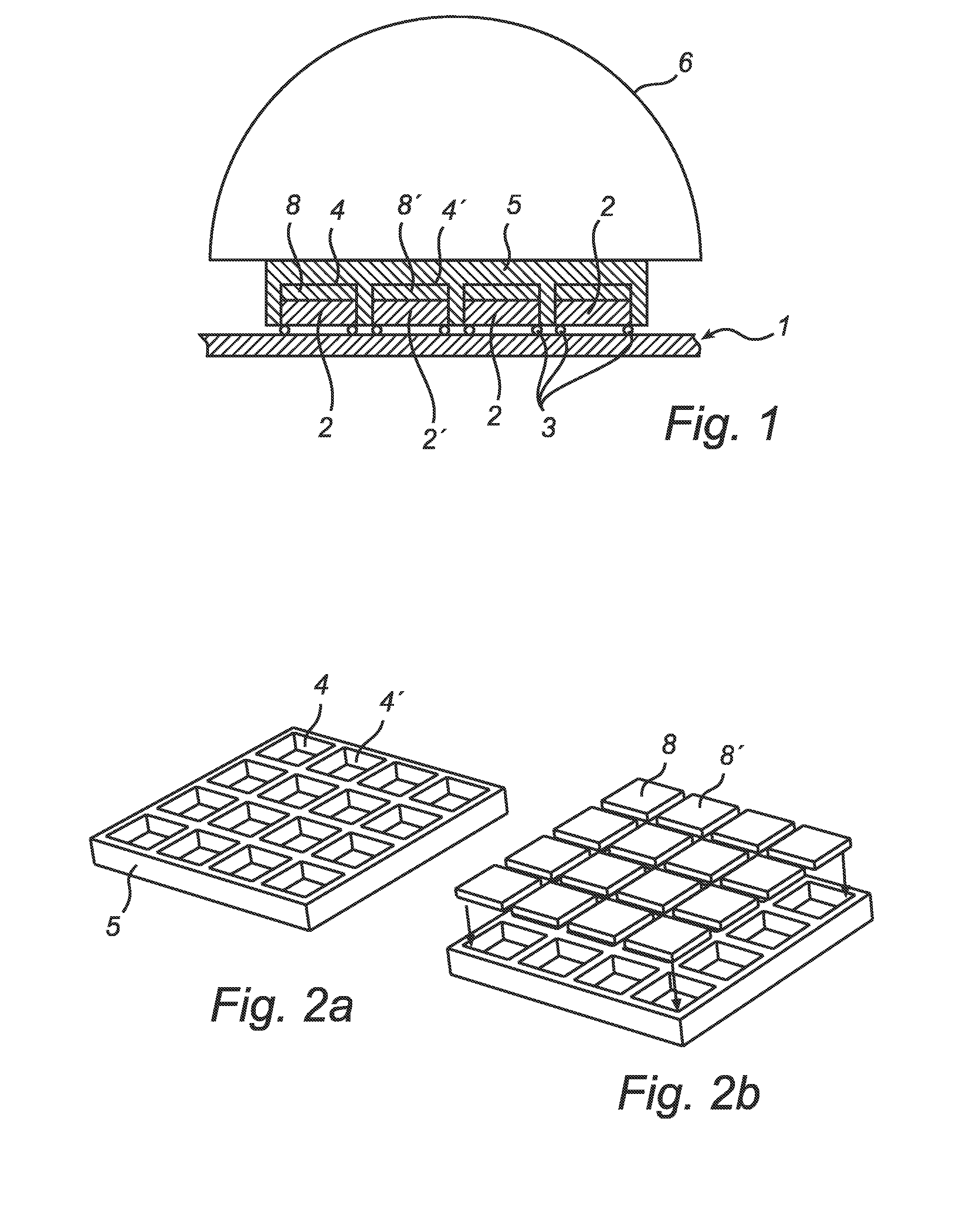
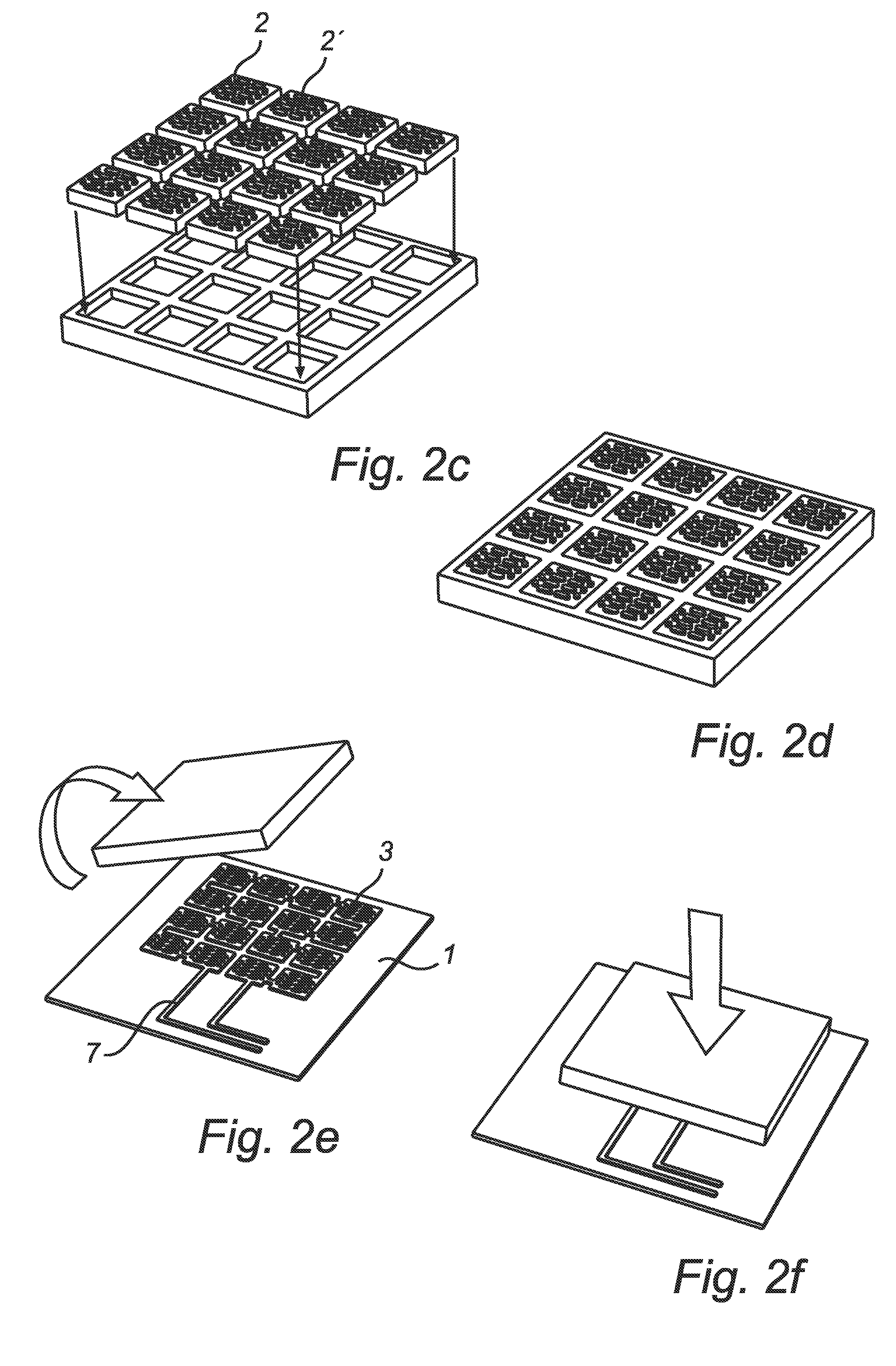
[0025]One exemplary embodiment of the present invention, as shown in FIG. 1, comprises a sub-mount 1 provided with a circuitry. An array of light-emitting diodes (LEDs) 2, 2′ is arranged on the circuitry, and each LED of the array is separately connected to the circuitry by metal bumps 3 at pre-determined positions.

[0026]Each LED 2, 2′ is arranged in a separate recess 4, 4′ in a housing 5 of a translucent glass material, and the location and the orientation of each LED 2, 2′ is determined by the walls of the corresponding recess 4, 4′.

[0027]Each LED comprises the active layers arranged on a crystalline substrate, through which light is emitted when the LEDs are active. The substrate is physically bonded to the housing in order to optically connect the LED with the housing.

[0028]Furthermore, a transparent hemisphere 6 is arranged on the housing 5 to spread the light emitted by the device. A preferred method for the manufacture of a light source of the present invention is outlined in...


PUM


Abstract

A light source comprising at least one light-emitting diode (2), which emits light, and a housing (5) arranged to receive at least a portion of said light is provided. The housing (5) comprises a translucent glass material and is provided with at least one recess (4) that comprises positioning and orientating means. The at least one light-emitting diode (2) is arranged in said at least one recess (4), is positioned and orientated by said positioning and orientating means and is bonded to said housing. By utilizing a fully inorganic approach for the housing, the temperature stability of the light source is improved.

Description

TECHNICAL FIELD[0001]The present invention relates to a light source comprising at least one light-emitting diode, which emits light, and a housing arranged to receive at least a portion of said light. The present invention further relates to a method for the manufacture of such a light source.TECHNICAL BACKGROUND[0002]Semiconductor light-emitting devices, such as light-emitting diodes (LEDs) and laser diodes (LDs), are among the most efficient and robust light sources currently available.[0003]Light extraction is a key issue for light emitting devices. A common problem of semiconductor light-emitting devices is that the efficiency with which light may be extracted from the device is reduced due to internal reflection in the interface between the device and the surroundings, followed by re-absorption of the reflected light in the device. The internal reflection is due to that the refractive index of the device materials is higher than the refractive index of the material in which th...

Claims


Application Information

Patent Timeline
Patent Type & Authority Applications(United States)
IPC IPC(8): H01J1/62H01J9/02H01L33/54H01L33/58H01L33/64
CPCH01L25/0753H01L33/54H01L33/58H01L33/64H01L2924/0002H01L2924/00
Inventor BECKERS, LUCAS JOHANNES ANNA MARIA
Owner KONINKLIJKE PHILIPS ELECTRONICS NV
Why Eureka
Try Eureka