Display device and preparation method thereof

A technology for display devices and substrates, which is used in the manufacture of semiconductor/solid-state devices, instruments, diodes, etc., and can solve the problems of low color temperature of white light, yellowish color point, and low blue-off intensity of display devices.

Pending Publication Date: 2019-09-06
BOE TECH GRP CO LTD +1
View PDF9 Cites 3 Cited by
  • Summary
  • Abstract
  • Description
  • Claims
  • Application Information

AI Technical Summary

Problems solved by technology

[0003] The present invention provides a display device to solve the problems of low blue-off inte

Method used


Image

  • Display device and preparation method thereof
  • Display device and preparation method thereof
  • Display device and preparation method thereof

Examples


Embodiment 1

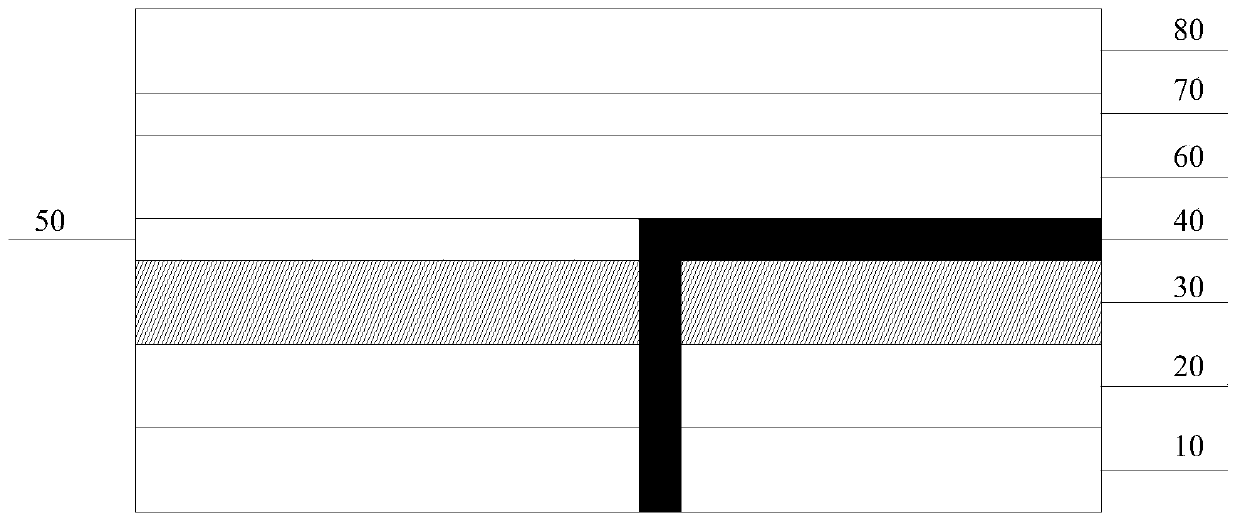
[0033] refer to figure 1 , shows a display device 10, the device includes:

[0034] Substrate 10, a planarization layer 20 covering the substrate 10, and a protective layer 30 covering the side of the planarization layer 20 away from the substrate 10; the protective layer 30 has thermal conductivity, transparency and insulation sex.

[0035] In the embodiment of the present invention, the substrate 10 is a TFT glass substrate. The planarization layer 20 is a resin material.

[0036] In the embodiment of the present invention, the protective layer 30 includes: a silicon dioxide thin film layer. Wherein, the silicon dioxide thin film layer can be prepared by a sol-gel method.

[0037] In the embodiment of the present invention, the protection layer 30 has good thermal conductivity, transparency and insulation.

[0038] Wherein, the thickness of the protective layer 30 includes: 1 μm-3 μm.

[0039] Wherein, the display device further includes: an anode layer 40, a pixel def...

Embodiment 2

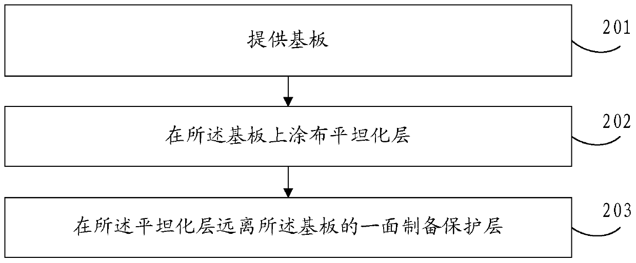
[0046] refer to figure 2 , showing a flowchart of steps of a method for manufacturing a display device provided by an embodiment of the present invention; the method specifically includes the following steps:

[0047] Step 201, providing a substrate.

[0048] In an embodiment of the present invention, the substrate includes: a TFT glass substrate.

[0049] Step 202, coating a planarization layer on the substrate.

[0050] In an embodiment of the present invention, the material of the planarization layer includes: a resin material.

[0051] Step 203 , preparing a protective layer on the side of the planarization layer away from the substrate.

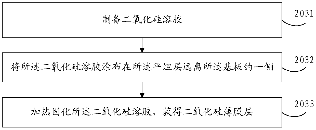
[0052] In the embodiment of the present invention, refer to image 3 , step 203 includes:

[0053] Step 2031, prepare silica sol;

[0054] Step 2032, coating the silica sol on the side of the planarization layer away from the substrate;

[0055] Step 2033, heating and curing the silica sol to obtain a silica film layer.

[0056]...


PUM

PropertyMeasurementUnit
Thicknessaaaaaaaaaa

Abstract

The embodiment of the invention provides a display device. The display device comprises a substrate, a planarized layer covering the substrate and a protective layer covering one side, deviating fromthe substrate, of the planarized layer; and the protective layer has thermal conductivity, transparency and insulativity. According to the embodiment of the invention, the protective layer with the thermal conductivity, transparency and insulativity covers the planarized layer, the planarized layer can be effectively protected, the planarized layer is prevented from deforming in a follow-up preparation process, loss of blue light in white light of the planarized layer is reduced, color temperature is increased, the white light is improved, and light emitting quality of the display device is improved.

Description

technical field [0001] The present invention relates to the field of display technology, in particular to a display device and a method for preparing the display device. Background technique [0002] In the current research field of liquid crystal display panels, the material of the planarization layer used in the display panel is usually a resin material, which is prone to shrinkage under a long-term thermal process or sputtering process, resulting in blue light transmission of the planarization layer. The reduction of the pass rate leads to low intensity of blue light in the white light plus color film panel, low color temperature of white light, and yellowish color point, but the prior art has not yet proposed a solution to this problem. Contents of the invention [0003] The invention provides a display device to solve the problems of low blue-off intensity, low white light color temperature and yellowish color point of the existing display device. [0004] One aspect...

Claims


Application Information

Patent Timeline
IPC IPC(8): G02F1/1333G02F1/13357
CPCG02F1/1333G02F1/133609H01L27/156H01L21/02164H01L21/02282H01L21/02216H01L27/1248H10K59/38H10K59/124H10K50/87H10K2102/331H01L27/1259H10K50/844H10K71/00H10K59/1201
Inventor 宋丽芳
Owner BOE TECH GRP CO LTD
Why Eureka
Try Eureka