A three-dimensional memory device and method of forming epitaxial structure in channel hole thereof

A technology of three-dimensional storage and epitaxial structure, which is applied in the direction of electric solid-state devices, semiconductor devices, electrical components, etc., can solve problems such as risk and leakage reliability, and achieve the effect of simplifying process difficulty and solving leakage and reliability risks

Active Publication Date: 2020-06-12
YANGTZE MEMORY TECH CO LTD
View PDF4 Cites 3 Cited by
  • Summary
  • Abstract
  • Description
  • Claims
  • Application Information

AI Technical Summary

Problems solved by technology

[0008] The invention provides a method for forming an epitaxial structure in a channel hole of a three-dimensional memory device, which can solve problems such as leakage and reliability risks caused by forming an epitaxial structure in an auxiliary region

Method used


Image

  • A three-dimensional memory device and method of forming epitaxial structure in channel hole thereof
  • A three-dimensional memory device and method of forming epitaxial structure in channel hole thereof
  • A three-dimensional memory device and method of forming epitaxial structure in channel hole thereof

Examples


Embodiment Construction

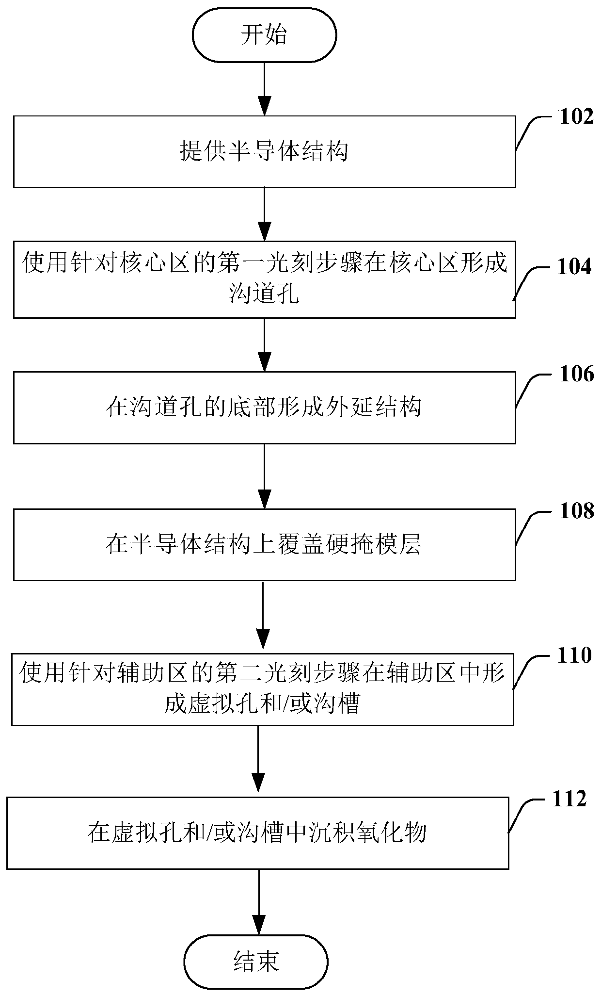
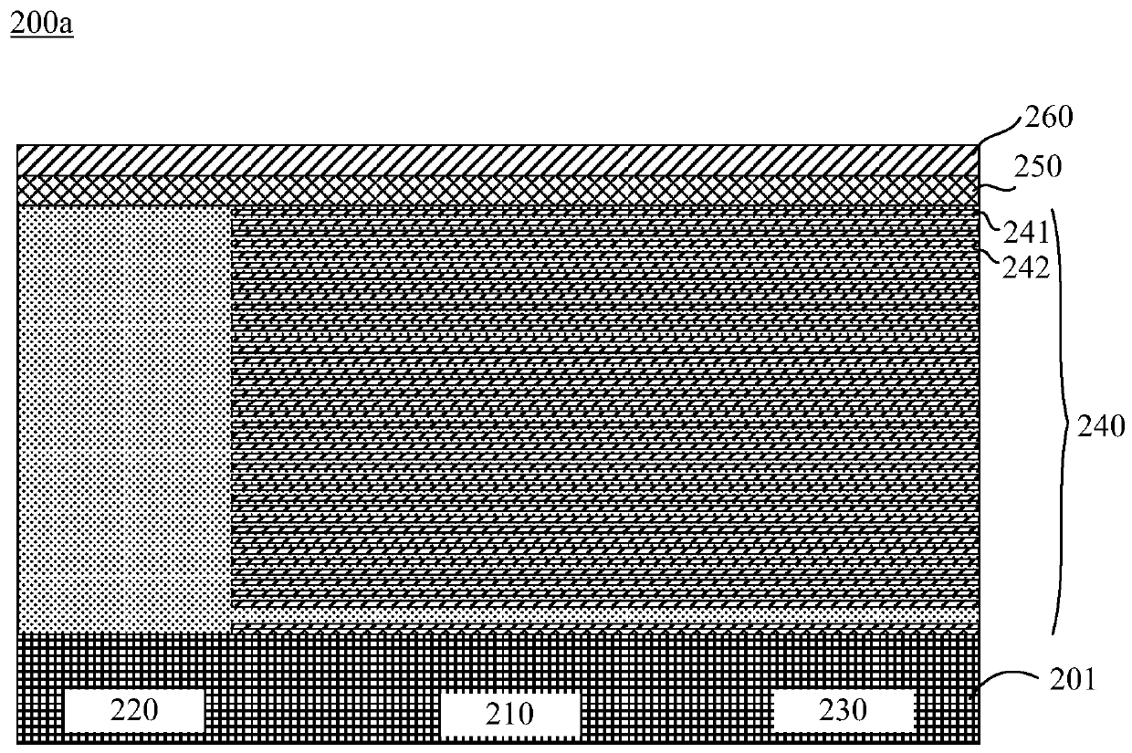
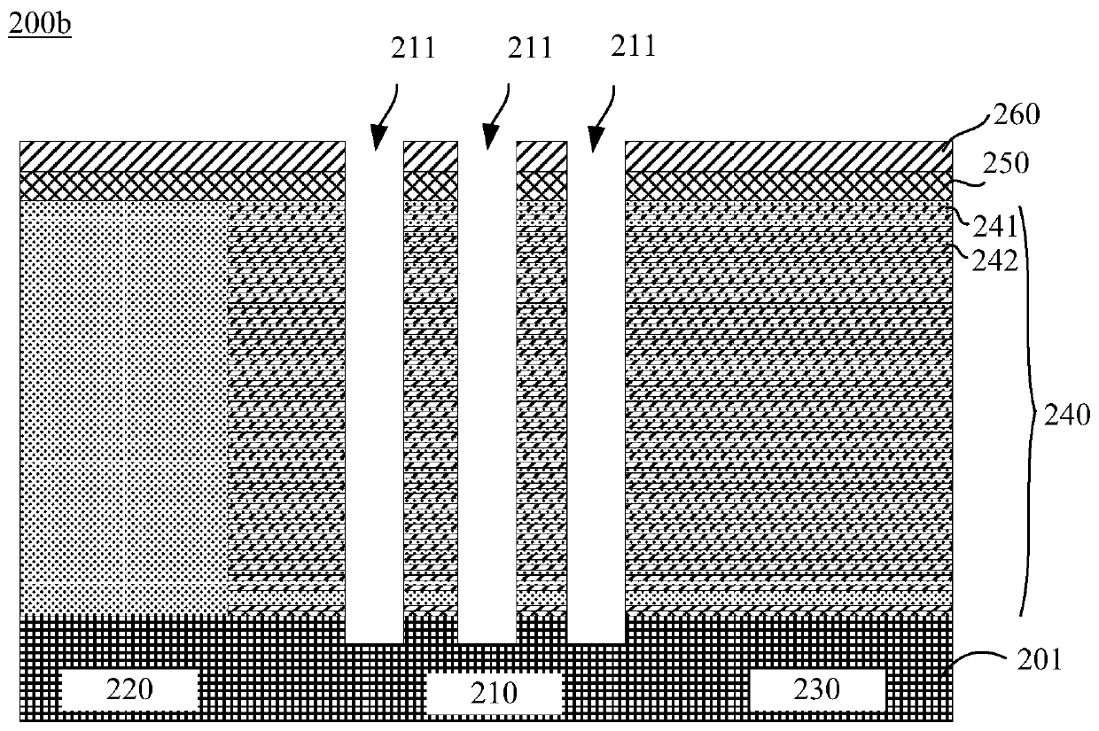
[0036] In order to make the above objects, features and advantages of the present invention more comprehensible, specific implementations of the present invention will be described in detail below in conjunction with the accompanying drawings.

[0037] In the following description, many specific details are set forth in order to fully understand the present invention, but the present invention can also be implemented in other ways than those described here, so the present invention is not limited by the specific embodiments disclosed below.

[0038] As indicated in this application and claims, the terms "a", "an", "an" and / or "the" do not refer to the singular and may include the plural unless the context clearly indicates an exception. Generally speaking, the terms "comprising" and "comprising" only suggest the inclusion of clearly identified steps and elements, and these steps and elements do not constitute an exclusive list, and the method or device may also contain other st...


PUM


Abstract

The invention relates to a method for forming an epitaxial structure in a channel hole of a three-dimensional memory device, the method comprises the following steps of: providing a semiconductor structure which comprises a core region and an auxiliary region; forming a channel hole in the core region using a first lithography step for the core region; forming an epitaxial structure at the bottomof the channel hole; and forming a dummy hole in the auxiliary region using a second lithography step for the auxiliary region. According to the invention, the epitaxial structure is only formed in the channel hole of the core region, and the epitaxial structure is not formed in the virtual hole and / or the groove of the auxiliary region, so that the risks of electric leakage and reliability causedby the formation of the epitaxial structure can be solved, and the process difficulty is simplified.

Description

[0001] This application was filed on March 14, 2018. The title of the invention is "Three-dimensional memory device and method for forming an epitaxial structure in its channel hole", and the application number is a divisional application of the Chinese invention patent application with the application number 201810209330.X. technical field [0002] The invention mainly relates to a semiconductor manufacturing method, in particular to a method for forming an epitaxial structure in a channel hole of a three-dimensional memory device, and the three-dimensional memory device. Background technique [0003] In order to overcome the limitations of two-dimensional memory devices, the industry has developed memory devices with a three-dimensional (3D) structure to increase integration density by three-dimensionally arranging memory cells on a substrate. [0004] A three-dimensional memory device is typically divided into a core region forming memory cells and an auxiliary region form...

Claims


Application Information

Patent Timeline
Patent Type & Authority Applications(China)
IPC IPC(8): H01L27/115H01L27/11582H01L27/1157H01L27/11573H01L27/11556H01L27/11524H01L27/11529
CPCH10B41/41H10B41/35H10B41/27H10B43/35H10B69/00H10B43/40H10B43/27
Inventor 杨号号吕震宇陈俊胡禺石陶谦董金文
Owner YANGTZE MEMORY TECH CO LTD
Why Eureka
Try Eureka