PCB demolding automatic cleaning device

A PCB circuit board, automatic cleaning technology, applied in the direction of cleaning flexible items, cleaning methods and utensils, cleaning methods using liquids, etc., can solve problems affecting the quality of PCB circuit boards, wiping, incomplete cleaning, etc.

Active Publication Date: 2020-10-23
广德万正电子科技有限公司
View PDF5 Cites 0 Cited by
  • Summary
  • Abstract
  • Description
  • Claims
  • Application Information

AI Technical Summary

Problems solved by technology

[0002] When etching and removing the film of PCB wet film board, and removing the solder resistance, it is necessary to stack the PCB circuit board parts in the water basin for immersion washing, and then produce them by machine. Since the PCB circuit board parts are stacked in the water basin for immersion washing, the PCB When the circuit boards are stacked, it is easy to cause scratches, which affects the quality of the PCB circuit boards, and the lines between the PCB circuit boards cannot be cleaned, and the cleaning is not thorough

Method used


Image

  • PCB demolding automatic cleaning device
  • PCB demolding automatic cleaning device
  • PCB demolding automatic cleaning device

Examples


Embodiment Construction

[0023] The following will clearly and completely describe the technical solutions in the embodiments of the present invention with reference to the accompanying drawings in the embodiments of the present invention. Obviously, the described embodiments are only some, not all, embodiments of the present invention. Based on the embodiments of the present invention, all other embodiments obtained by persons of ordinary skill in the art without creative efforts fall within the protection scope of the present invention.

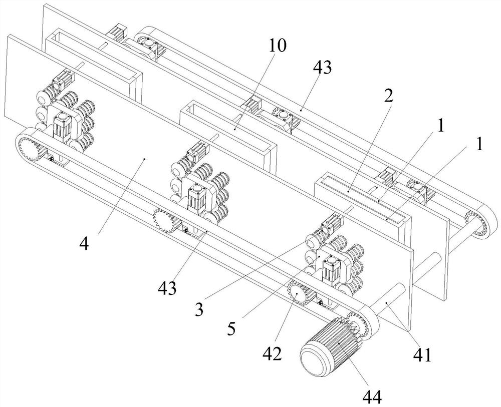
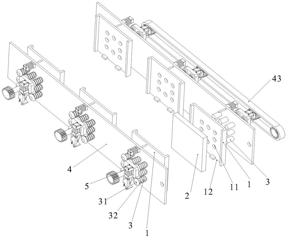
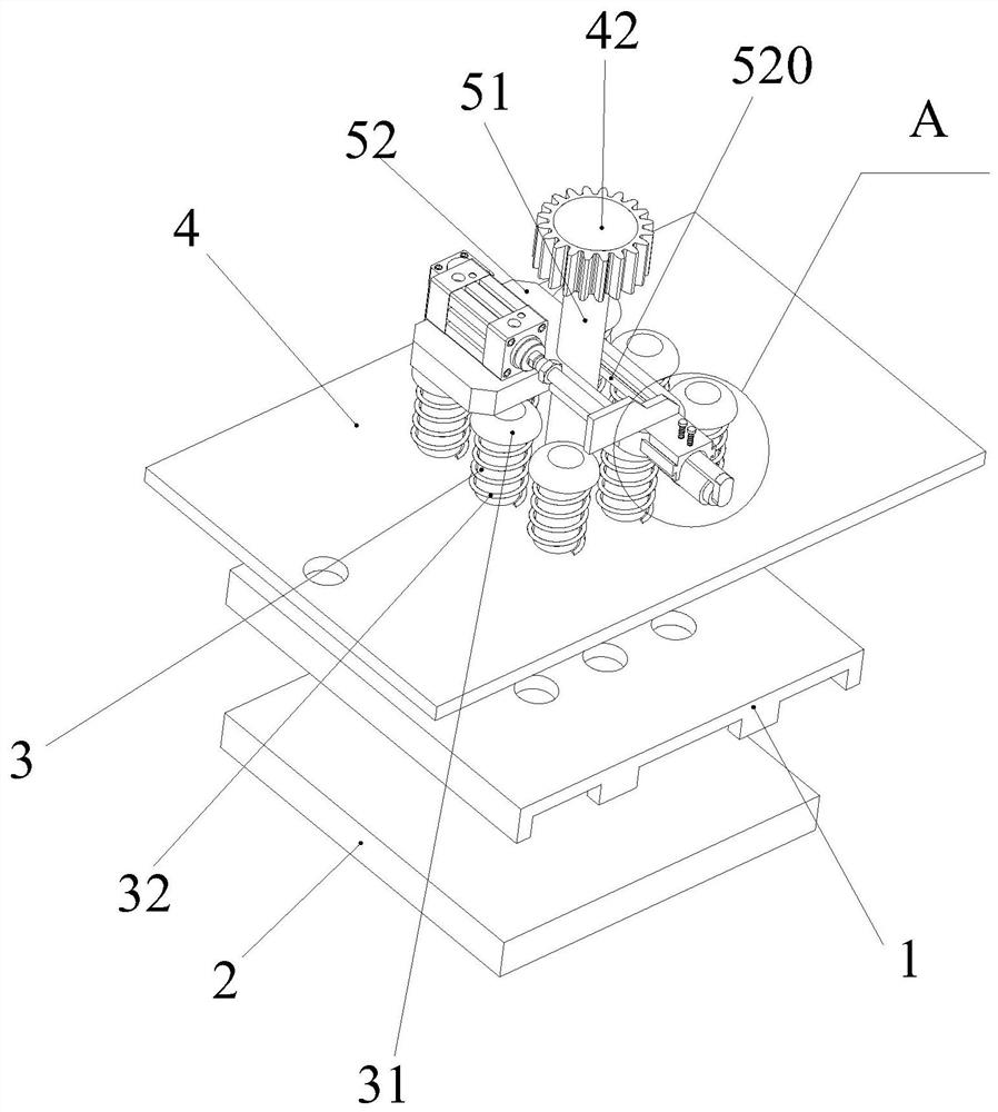
[0024] Such as figure 1 and figure 2 As shown in the figure, an automatic cleaning device for removing film from a PCB circuit board includes several sets of clamping shells 1 that are mirror images of each other. 10, wherein the storage compartment 10 is used to place the PCB circuit board 2 with cleaning;

[0025] Above the storage bins 10 are provided with nozzles (the nozzles are not shown in the illustration of this embodiment), and the nozzles are used to ...


PUM


Abstract

The invention belongs to the field of PCBs and discloses a PCB demolding automatic cleaning device. The PCB demolding automatic cleaning device comprises a plurality of clamping shells distributed ina mirroring mode. The clamping shells distributed in the mirroring mode are mutually clamped to form storage chambers with open top ends. The storage chambers are used for storing PCBs to be cleaned.Spray heads are arranged above the storage chambers. The sidewalls of the clamping shells are provided with moving holes distributed in an array mode. Clamping columns are inserted into the moving holes. The clamping columns are used for clamping the PCBs located in the storage chambers. During the process of spraying and washing the PCBs, the different clamping columns intermittently clamp the PCBs. The single PCBs are cleaned in a spraying and washing mode, and the problem that wire spaces of the PCBs cannot be cleaned is avoided. In the cleaning process, the spray heads can wash the contactparts of the PCBs and the clamped PCBs to prevent sundries from existing in the clamped parts of the PCBs due to clamping washing.

Description

technical field [0001] The invention belongs to the field of PCB circuit boards, and in particular relates to an automatic cleaning device for removing film from a PCB circuit board. Background technique [0002] When etching and removing the film of PCB wet film board, and removing the solder resistance, it is necessary to stack the PCB circuit board parts in the water basin for immersion washing, and then produce them by machine. Since the PCB circuit board parts are stacked in the water basin for immersion washing, the PCB When the circuit board parts are stacked, it is easy to cause scratches, which affects the quality of the PCB circuit board, and the lines between the PCB circuit board parts cannot be cleaned, and the cleaning is not thorough. Contents of the invention [0003] Aiming at the deficiencies of the prior art, the purpose of the present invention is to provide an automatic cleaning device for removing film from PCB circuit boards, which solves the technic...

Claims


Application Information

Patent Timeline
Patent Type & Authority Applications(China)
IPC IPC(8): B08B11/02B08B3/02
CPCB08B3/02B08B11/02
Inventor 董颖辉葛庆新刘媛张俊涛陶继宏
Owner 广德万正电子科技有限公司
Why Eureka
Try Eureka