A kind of silicon carbon film negative electrode with graphene as skeleton and preparation method thereof
A graphene skeleton and graphene technology, applied in the direction of negative electrodes, battery electrodes, active material electrodes, etc., can solve the problems of large volume change, low cycle life, and SEI film generation, and overcome the problems of silicon negative electrode materials. Convenience, the effect of a simple method
- Summary
- Abstract
- Description
- Claims
- Application Information
AI Technical Summary
Problems solved by technology
Method used
Image

Examples
Embodiment 1
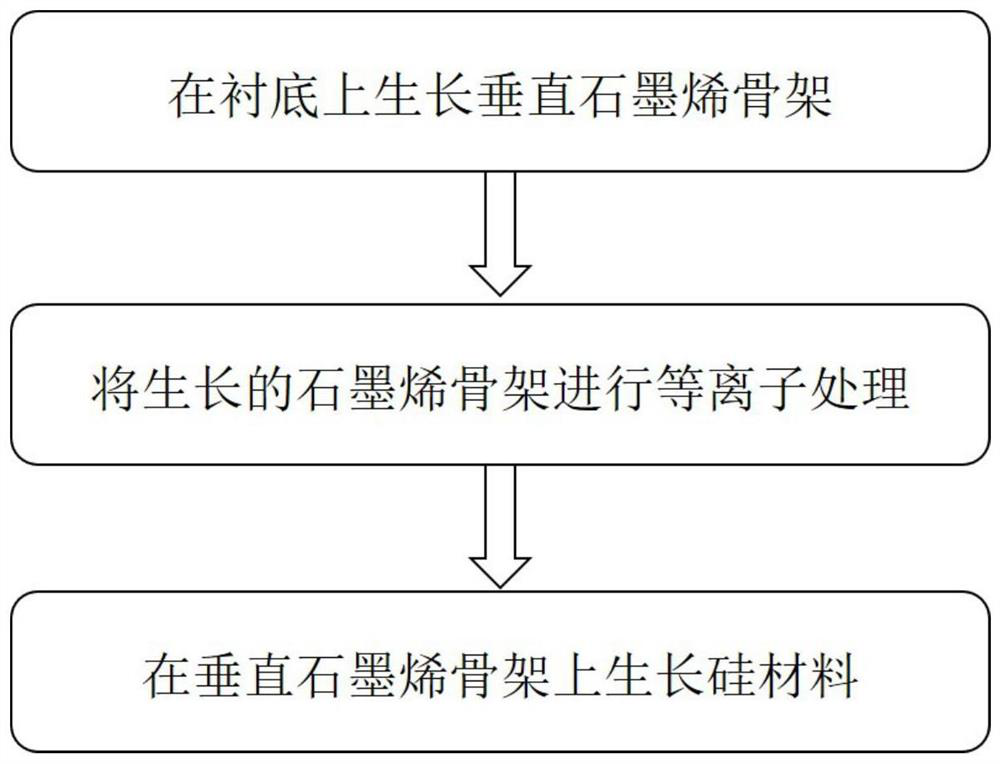
[0033] This embodiment discloses the preparation method of the silicon carbon thin film negative electrode with graphene as the skeleton of the present invention, and its process flow chart is as attached figure 1 As shown, specifically:
[0034] Step 1. Use radio frequency plasma enhanced chemical vapor deposition (RF-PECVD) to grow a vertical graphene framework on the substrate copper foil:
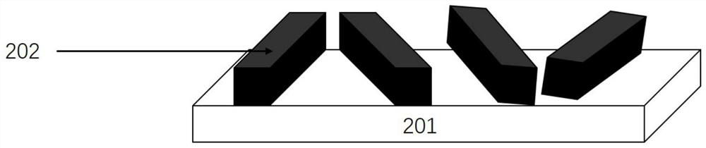
[0035] as attached figure 2 shown, with pure CH 4 As a reaction gas, a vertical graphene framework 202 is deposited on a clean substrate 201 . The operating conditions are: substrate temperature 400°C, gas CH 4 The flow rate is 50sccm, H 2 The flow rate is 500sccm, the pressure is 0.4mbar, and the deposition power is 50mW / cm 2 , the length of the prepared vertical graphene is about 500 nm.
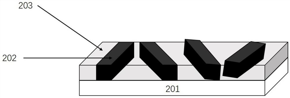
[0036] Step 2. Plasma treatment of the grown vertical graphene skeleton:
[0037] Stop CH 4 , H 2 The flow rate is adjusted to 100sccm, and the RF power is adjusted to 20mW / cm 2 , process...
Embodiment 2
[0041] This example discloses the preparation method of the silicon-carbon thin film negative electrode with graphene as the skeleton of the present invention. Compared with Example 1, the carbon source of this example is ethylene, and the rest of the conditions are the same, and the amorphous silicon layer is prepared. The thickness is about 500nm.
Embodiment 3
[0043] This example discloses the preparation method of the silicon-carbon thin film negative electrode with graphene as the skeleton of the present invention. Compared with Example 1, the carbon source of this example is ethanol, and the rest of the conditions are the same, and the amorphous silicon layer is prepared. The thickness is about 500nm.
PUM
| Property | Measurement | Unit |
|---|---|---|
| length | aaaaa | aaaaa |
| length | aaaaa | aaaaa |
Abstract
Description
Claims
Application Information
 - R&D
- Intellectual Property
- Life Sciences
- Materials
- Tech Scout
- Unparalleled Data Quality
- Higher Quality Content
- 60% Fewer Hallucinations
Browse by: Latest US Patents, China's latest patents, Technical Efficacy Thesaurus, Application Domain, Technology Topic, Popular Technical Reports.
© 2025 PatSnap. All rights reserved.Legal|Privacy policy|Modern Slavery Act Transparency Statement|Sitemap|About US| Contact US: help@patsnap.com