A chip cleaning device and cleaning method

A chip cleaning and chip technology, used in cleaning methods and utensils, cleaning methods using liquids, chemical instruments and methods, etc., can solve the problems of a large number of bumps on the chip surface, damage, and small size, and achieve semi-automatic cleaning. , Improve cleaning efficiency and reduce damage

Active Publication Date: 2021-06-04
北京智创芯源科技有限公司
View PDF0 Cites 0 Cited by
  • Summary
  • Abstract
  • Description
  • Claims
  • Application Information

AI Technical Summary

Problems solved by technology

[0004] Due to the large number of bumps on the surface of the chip, small size, and made of soft metal, it is easy to be scratched and damaged by tweezers during the cleaning process; optoelectronic device chips are usually made of some relatively brittle materials, which are extremely fragile. Easy to be damaged due to excessive clamping force, resulting in chip scrapping

Method used


Image

  • A chip cleaning device and cleaning method
  • A chip cleaning device and cleaning method
  • A chip cleaning device and cleaning method

Examples


Embodiment 1

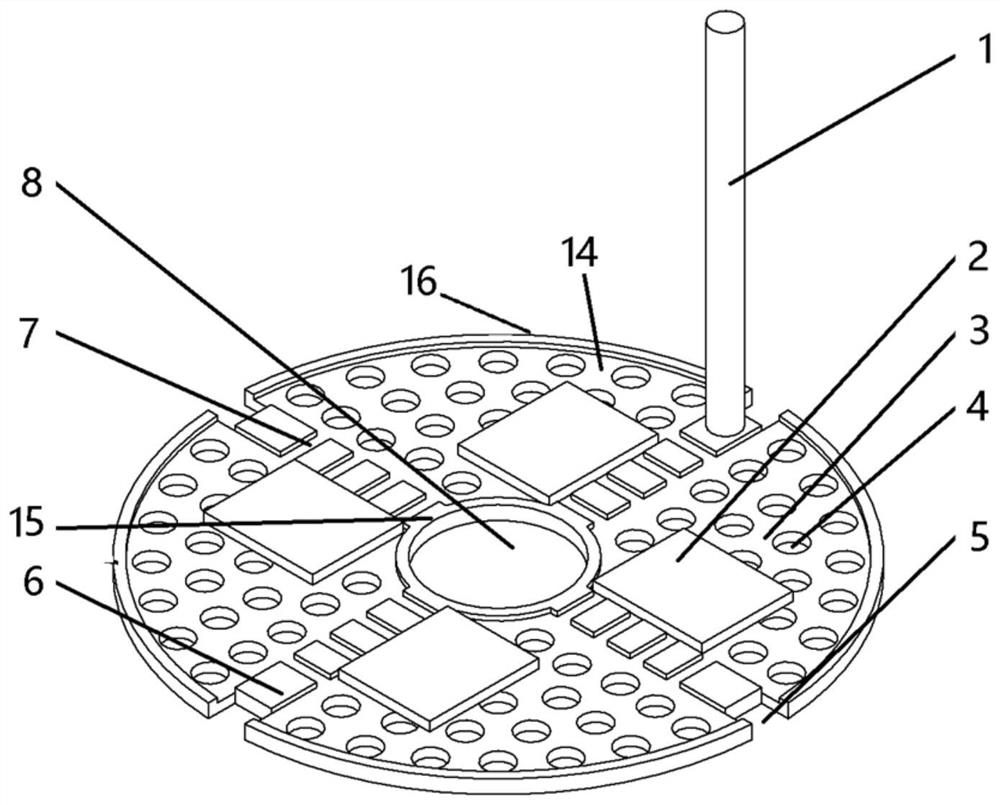
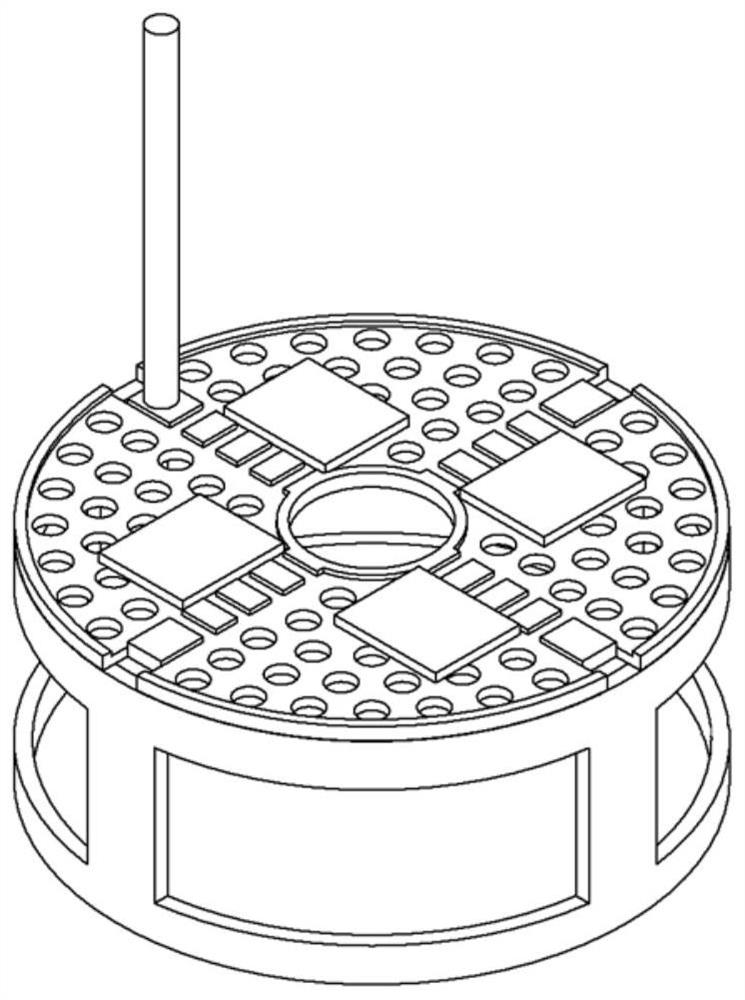
[0045] see figure 1 , the carrying portion in the present embodiment is a carrying plate 14, and the bottom wall of the carrying plate 14 is evenly distributed with a plurality of circular through-holes 4 to allow the solvent to flow up and down, and a guide hole 8 is provided in the center of the carrying plate 14, The outer edge of the guide hole 8 is provided with a guide hole boss 15 that is higher than the bottom wall of the carrier tray 14 , and the outer edge of the carrier tray 14 is provided with a carrier tray boss 16 . Wherein, the isolation part includes four isolation strips 6 arranged on the carrier plate 14 , one end of each isolation band 6 is connected to the boss 15 of the flow guide hole, and the other end extends to the outer edge of the carrier plate 14 . The four isolation strips 6 are distributed on the carrier tray 14 in a diverging shape, and divide the carrier tray 14 into four cleaning units 3 with fan-shaped structures. By placing each chip 2 in an...

Embodiment 2

[0051] The structure of the chip cleaning device in this embodiment is basically the same as that in Embodiment 1, the difference is that the stirrer in this embodiment is a mechanical stirrer with stirring paddles arranged above the carrying plate, and the fluid acts on the stirring paddles Down, the rotating flow conducts from top to bottom. It is not necessary to set up diversion holes on the carrier plate, and at the same time, it is also possible to place the carrier plate directly on the bottom of the container filled with solvent to meet the requirements of the solvent in the rotating flow state. Technical requirements for scour cleaning.

[0052] The present invention also provides a method for cleaning chips implemented by the above-mentioned chip cleaning device. Specifically, the cleaning of chips is explained in the form of a magnetic stirrer in Example 1:

[0053] see Figure 5a-5c , and combined with figure 1 , first place the support 10 and the rotating magnet...


PUM


Abstract

The invention discloses a chip cleaning device, comprising: a carrying part, which has a plurality of cleaning units separated from each other, and the cleaning units are used to place chips; The chip on the carrying part is submerged in or lifted out of the solvent, and the solvent is used to clean the chip; the stirrer is used to make the solvent flow to clean the chip. By placing the chip on the carrier during the cleaning process, and immersing the carrier and the chip in the solvent through the hand-held part, or lifting it out of the solvent, there is no need to manually clamp the chip, which reduces the damage it receives when cleaning in the solvent ;By separating the carrier part into multiple cleaning units that are separated from each other, multiple chips can be processed in one cleaning process, which improves the cleaning efficiency; the solvent flows through the agitator, instead of manual shaking and rinsing in the solvent, effectively realizing Semi-automatic cleaning of chips.

Description

technical field [0001] The invention relates to the technical field of photoelectric devices, in particular to a chip cleaning device and a cleaning method. Background technique [0002] Flip-chip interconnection technology is a high-precision, high-reliability technology that is widely used in the packaging of optoelectronic devices and can realize the miniaturization and mass production of optoelectronic devices. Optoelectronic devices used for flip-chip interconnection have several metal bump arrays for electrical communication prepared on the surface. The size of the bumps is small, with a diameter between 5um and 100um; the bumps usually appear in the form of a matrix, and the number It can range from thousands to millions. In order to ensure the quality of flip-chip interconnection, devices must be cleaned before interconnection. [0003] The existing chip cleaning process is as follows: the operator holds the chip to be cleaned with tweezers, places it in a containe...

Claims


Application Information

Patent Timeline
Patent Type & Authority Patents(China)
IPC IPC(8): H01L21/673H01L21/67H01L21/02B08B3/10
CPCB08B3/102H01L21/02068H01L21/67057H01L21/67333
Inventor 不公告发明人
Owner 北京智创芯源科技有限公司
Why Eureka
Try Eureka