Method for detecting pupil plane transmittance distribution of photoetching equipment

A technology of lithography equipment and detection method, which is applied in the detection field of pupil surface transmittance distribution, can solve the problems of cumbersome operation and long detection time, and achieve the effects of ensuring imaging contrast, short detection time, and convenient detection process

Active Publication Date: 2020-12-29
SHANGHAI MICRO ELECTRONICS EQUIP (GRP) CO LTD
View PDF5 Cites 0 Cited by
  • Summary
  • Abstract
  • Description
  • Claims
  • Application Information

AI Technical Summary

Problems solved by technology

[0005] The purpose of the present invention is to provide a method for detecting the pupil transmittance distribution of lithography e

Method used


Image

  • Method for detecting pupil plane transmittance distribution of photoetching equipment
  • Method for detecting pupil plane transmittance distribution of photoetching equipment
  • Method for detecting pupil plane transmittance distribution of photoetching equipment

Examples


Embodiment Construction
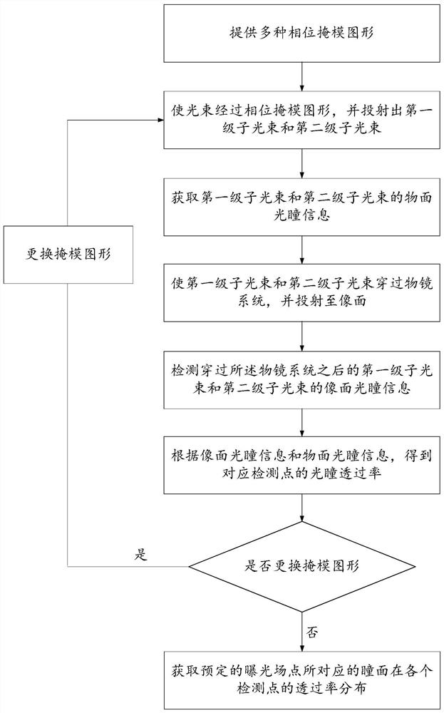
[0052] The core idea of ​​the present invention is to provide a method for detecting pupil transmittance distribution of lithography equipment, including:

[0053] Provide a variety of phase mask patterns;

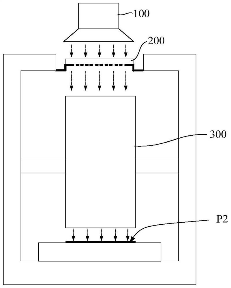
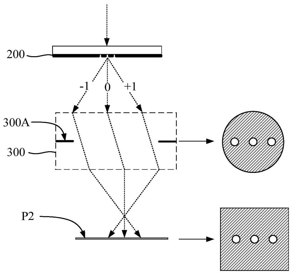
[0054]A light beam is provided by an illumination system, and the light beam is sequentially passed through each phase mask pattern to project a first-level sub-beam and a second-level sub-beam, wherein the second-level sub-beams projected by different phase mask patterns correspond to at different locations on the object plane;

[0055] obtaining object plane pupil information of the first-order sub-beams and the second-order sub-beams projected by each phase mask pattern before passing through the objective lens system;

[0056] The first-order sub-beams and the second-order sub-beams projected from each phase mask pattern are sequentially passed through the objective lens system to be projected onto the image plane, and the first-order sub-beams and the second-order su...


PUM


Abstract

The invention provides a method for detecting pupil plane transmittance distribution of photoetching equipment. According to the method, multiple phase mask patterns are provided, and the second-stagesub-beams projected from different phase mask patterns are enabled to respectively correspond to different positions of the pupil plane of the imaging system, so pupil transmittance detection can beperformed on multiple detection points on the pupil plane of the imaging system, and transmittance distribution of the whole pupil plane is further obtained. Namely, the pupil plane transmittance distribution detection method provided by the invention is convenient in detection process and relatively short in detection duration, and is beneficial to realizing that the photoetching equipment executes the detection process in a short period so as to monitor the pupil transmittance state of the photoetching equipment in time.

Description

technical field [0001] The invention relates to the technical field of semiconductors, in particular to a method for detecting pupil transmittance distribution of photolithography equipment. Background technique [0002] With the development of projection lithography technology, the performance of the projection optical system of lithography equipment has been gradually improved. At present, lithography equipment has been successfully applied in the field of integrated circuit manufacturing with submicron and deep submicron resolution. And, in order to adapt to the technological requirements of integrated circuit manufacturing breaking through 45nm, 32nm and 22nm technology nodes, lithography equipment must also improve its imaging resolution, and one of the ways to improve imaging resolution is to increase the objective lens system of lithography equipment. Numerical aperture NA, however, using an objective system with a large numerical aperture will cause the effect of the...

Claims


Application Information

Patent Timeline
IPC IPC(8): G03F7/20
CPCG03F7/70308G03F7/70591G03F7/7085
Inventor 孙文凤
Owner SHANGHAI MICRO ELECTRONICS EQUIP (GRP) CO LTD
Why Eureka
Try Eureka