Supercharge Your Innovation With Domain-Expert AI Agents!

Circuit substrate, display panel and display device

A circuit substrate and control display technology, which is applied in the direction of identification devices, static indicators, instruments, etc., can solve the problems of poor picture display effect at splicing places, achieve the effect of reducing frame size and avoiding occupying frame space

Active Publication Date: 2021-01-05
YUNGU GUAN TECH CO LTD
View PDF18 Cites 2 Cited by
  • Summary
  • Abstract
  • Description
  • Claims
  • Application Information

AI Technical Summary

Problems solved by technology

[0003] Usually, in order to realize large-size and ultra-large-size displays, multiple Micro LED display panels need to be spliced ​​together, but due to the borders of the Micro LED display panels, the picture display effect at the splicing place is not good

Method used


Image

  • Circuit substrate, display panel and display device
  • Circuit substrate, display panel and display device
  • Circuit substrate, display panel and display device

Examples


Embodiment Construction

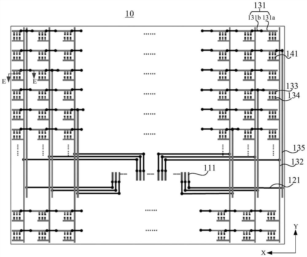
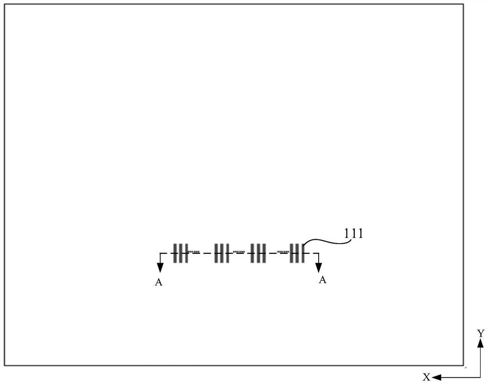
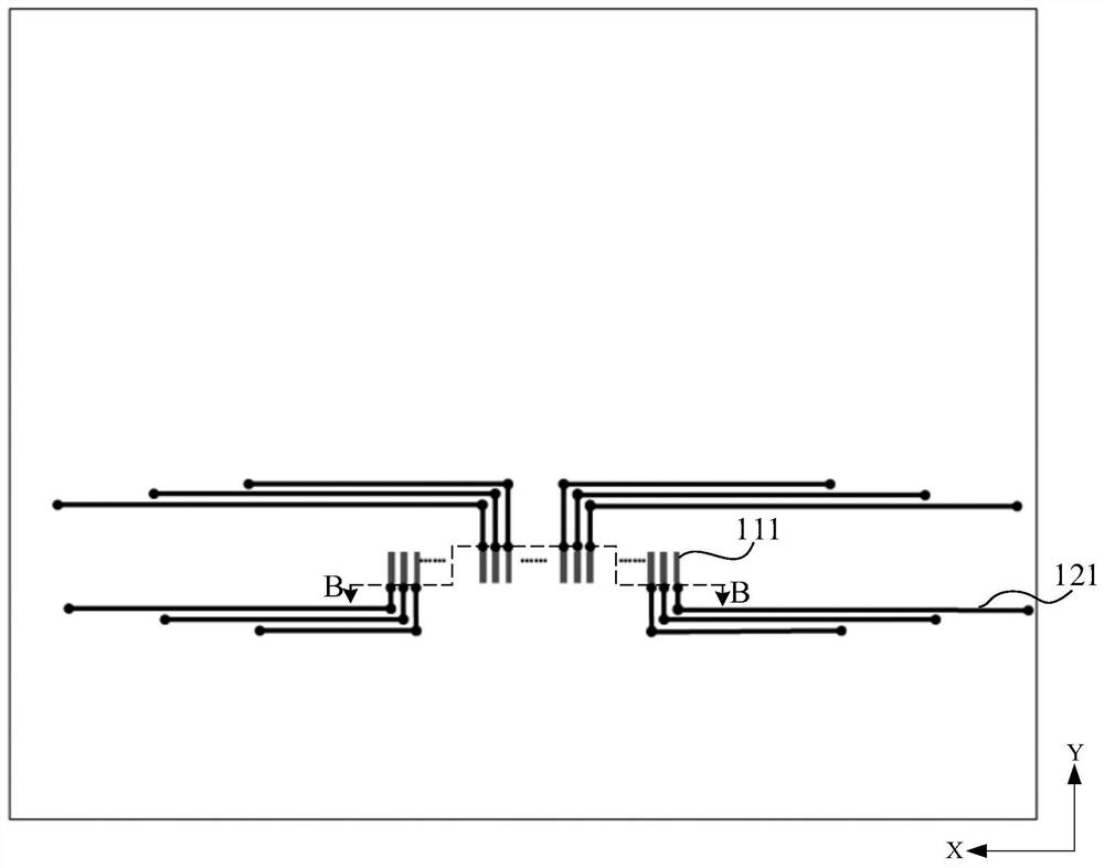
[0031]The features and exemplary embodiments of various aspects of the present invention will be described in detail below. In order to make the objectives, technical solutions, and advantages of the present invention clearer, the following further describes the present invention in detail with reference to the accompanying drawings and specific embodiments. It should be understood that the specific embodiments described herein are only configured to explain the present invention, and are not configured to limit the present invention. For those skilled in the art, the present invention can be implemented without some of these specific details. The following description of the embodiments is only to provide a better understanding of the present invention by showing examples of the present invention.

[0032]It should be noted that in this article, relational terms such as first and second are only used to distinguish one entity or operation from another entity or operation, and do not n...


PUM


Abstract

The invention discloses a circuit substrate, a display panel and a display device. The circuit substrate is used for controlling the display panel to display, the circuit substrate is provided with afirst area, the first area corresponds to a display area of the display panel to be controlled, the circuit substrate comprises a driving lead layer and an electrode layer which are arranged in an insulating mode, the driving lead layer comprises a plurality of driving leads, and the driving leads can be electrically connected with an external driving chip; the electrode layer comprises a row electrode lead, a column electrode lead, a first electrode and a second electrode, wherein the first electrode and the second electrode are arranged in pairs and used for binding an external device, and adriving lead of the driving lead layer is located in the first area. According to the circuit substrate disclosed by the invention, the driving leads are arranged on the back side of one side, whichcan be bound with the external device, of the electrode layer, so that the external driving chip can be bound on the back surface of the electrode layer, the driving chip is prevented from occupying frame space, and the frame size can be reduced.

Description

Technical field[0001]The invention belongs to the field of display technology, and particularly relates to a circuit substrate, a display panel and a display device.Background technique[0002]Micro LED (Micro LED) technology refers to the technology of integrating high-density and small-size LED arrays on a substrate. Since Micro LED displays are self-luminous displays, they have better material stability and longer lifespan than OLEDs. Advantages, with greater application potential.[0003]Generally, in order to realize large-size and super-size displays, multiple Micro LED display panels need to be spliced ​​together. However, due to the frame of the Micro LED display panels, the picture display effect at the splicing site is not good.[0004]Therefore, how to reduce the frame of the Micro LED display panel becomes an urgent problem to be solved.Summary of the invention[0005]The embodiments of the present invention provide a circuit substrate, a display panel, and a display device, aim...

Claims


Application Information

Patent Timeline
Patent Type & Authority Applications(China)
IPC IPC(8): G09F9/33G09G3/32
CPCG09F9/33G09G3/32G09G2300/0426
Inventor 邢汝博张志豪
Owner YUNGU GUAN TECH CO LTD
Features
  • R&D
  • Intellectual Property
  • Life Sciences
  • Materials
  • Tech Scout
  • Unparalleled Data Quality
  • Higher Quality Content
  • 60% Fewer Hallucinations
Learn More