A seamless splicing correction method and device for an LED display

An LED display, seamless splicing technology, applied in static indicators, instruments, etc., can solve problems such as poor calibration effect on large screens, detection of missing, limited pixels on graphics cards, and achieve uniform brightness and eliminate brightness measurement errors. Effect

Active Publication Date: 2022-02-08
SHENZHEN LIDING PHOTOELECTRIC TECH
View PDF0 Cites 0 Cited by
  • Summary
  • Abstract
  • Description
  • Claims
  • Application Information

AI Technical Summary

Problems solved by technology

[0002] The LED display is usually composed of multiple cabinets, and multiple sending cards are required to transmit various command parameters and video data issued by the control terminal. For example, a 64k LED display usually requires 64 Sending cards are used for transmission. At present, in order to calibrate each LED cabinet, it is necessary to use the card detection method to detect all sending cards. However, due to the large number of sending cards, there may be detection artifacts in the process of detecting sending cards. and the graphics card of the control terminal has limited pixels, which cannot be satisfied with the above-mentioned large screen body, so it will not be possible to generate the correction coefficient of the entire LED display at one time through the control terminal; in view of the above two problems, the current The solution is: first divide the LED display screen into a certain number of LED cabinets, then obtain the correction images corresponding to each LED cabinet, and finally correct the LED display screen by correcting the images, but due to the gap between the LED cabinets After being divided, it is easy to form a bright and dark line at the junction of the LED cabinet in the calibration image corresponding to the LED cabinet, so it will directly affect the calibration effect of the entire LED display
Therefore, those skilled in the art urgently need to find a new technical solution to solve the problem of poor correction effect of the above-mentioned large screen

Method used


Image

  • A seamless splicing correction method and device for an LED display
  • A seamless splicing correction method and device for an LED display
  • A seamless splicing correction method and device for an LED display

Examples


Embodiment Construction

[0065] DETAILED DESCRIPTION OF THE PREFERRED EMBODIMENTS It should be understood that the specific embodiments described herein are intended to illustrate and explain the disclosure and is not intended to limit the disclosure.

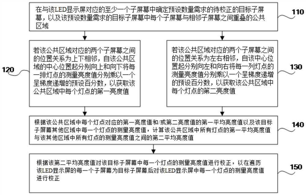
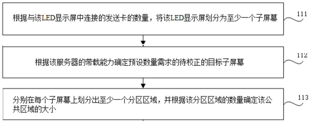
[0066] figure 1 It is a flow chart of a seamless splicing correction method of an LED display according to an exemplary embodiment, such as figure 1 As shown, it is applied to the server, which includes:

[0067] The target application scenario according to various embodiments in the present disclosure is first introduced, and the target application scenario includes a server, which is a computing function and can respond And send a service request server. The server can be, for example, a server in a control terminal.

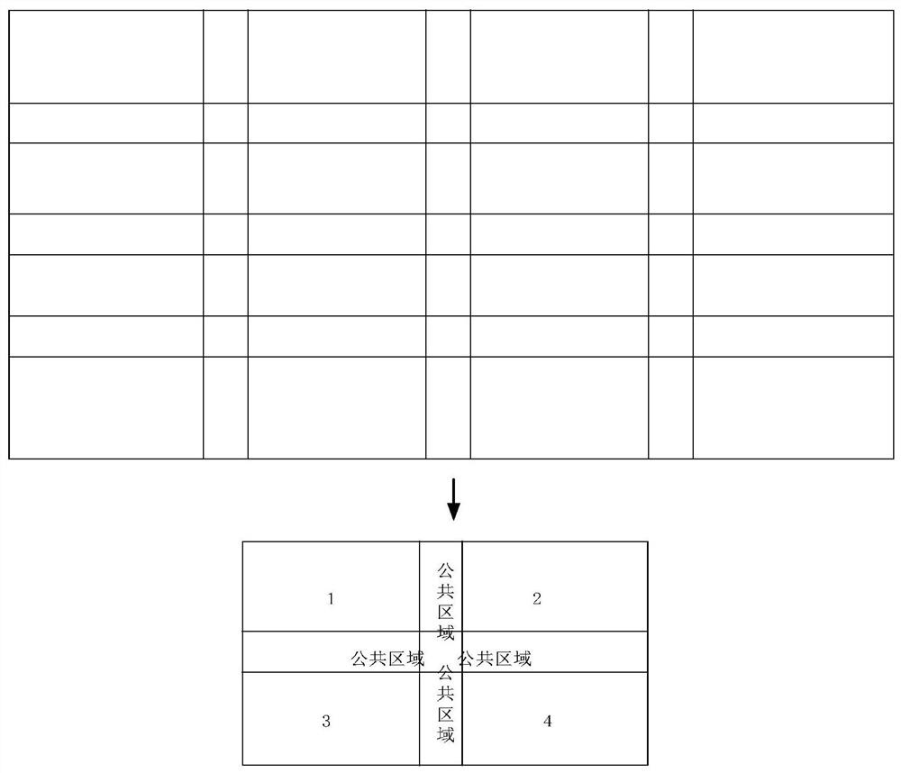
[0068] In step 110, the target sub-screen to be corrected in the preset quantity requirement is determined in at least one sub-screen corresponding to the LED display, and each sub-screen and the adjacent sub-screen in the target sub-scre...


PUM


Abstract

The disclosure of the present invention relates to a method and device for seamless splicing calibration of LED display screens, the method comprising: determining a preset number of target sub-screens to be corrected and public sub-screens in at least one sub-screen corresponding to the LED display screen area; from the center position of the public area, multiply the measured brightness value of each row of light points by a preset percentage that increases in a gradient from up and down or left and right; calculate the difference between all light points in other areas of the target sub-screen and The second average brightness value between the first average brightness values ​​of all light points in the public area; according to the second average brightness value, the measured brightness value of each light point in the target sub-screen is corrected so that after traversing the LED display screen Calibrate all light points. This solution adjusts the brightness of the public area by gradient, and then adjusts the brightness of the sub-screen through the correction coefficient of the public area. The correction process is not limited by the maximum load capacity of the PC and the shape of the LED display, so that the adjusted brightness transition is more uniform.

Description

Technical field [0001] The present invention discloses the correctional technique of the LED display screen, and in particular, to a seamless splicing correction method and apparatus for an LED display screen. Background technique [0002] The LED display is typically composed of multiple boxes and requires multiple transmit cards to transmit various instruction parameters and video data issued by the control terminal, such as a 64K LED display, usually need to use 64 Zhang Send Card for transmission, currently in order to correct each LED cabinet, you need to use the probe card to detect all send cards, but because the number of send cards is more, there may be probation legacy in the process of detecting the sender. The problem of falling; and the pixel loaded by the control terminal is limited, it cannot be satisfied with the above-mentioned large screen body, so it will not be able to generate the correction coefficient of the entire LED display by the control terminal; for t...

Claims


Application Information

Patent Timeline
Patent Type & Authority Patents(China)
IPC IPC(8): G09G3/32
CPCG09G3/32G09G2320/0626
Inventor 何志民阮诗安
Owner SHENZHEN LIDING PHOTOELECTRIC TECH
Why Eureka
Try Eureka