

Display driving method, circuit and display panel
A display driver and display panel technology, which is applied to static indicators, instruments, etc., can solve problems such as brightness differences and affect display effects, and achieve the effects of small brightness differences, improved display brightness, and improved charging efficiency
- Summary
- Abstract
- Description
- Claims
- Application Information
AI Technical Summary
Problems solved by technology
Method used
Image

Examples
Embodiment 1
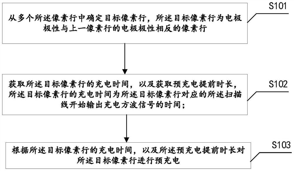
[0034] In order to solve the problem in the related art that there is a difference in brightness between adjacent pixel rows in the display panel, and the phenomenon of bright and dark lines appears on the display panel, which affects the display effect, please refer to figure 1 , figure 1 A schematic diagram of a display driving method provided in an embodiment of the present application, the method includes:
[0035] S101, determining a target pixel row from a plurality of the pixel rows, and the target pixel row has a pixel row whose electrode polarity is opposite to the electrode polarity of the previous pixel row;
[0036] S102, acquiring the charging time of the target pixel row, and acquiring the pre-charging advance duration, where the charging time of the target pixel row is the time when the scan line corresponding to the target pixel row starts to output a charging square wave signal;
[0037] S103. Precharge the target pixel row according to the charging time of t...
Embodiment 2
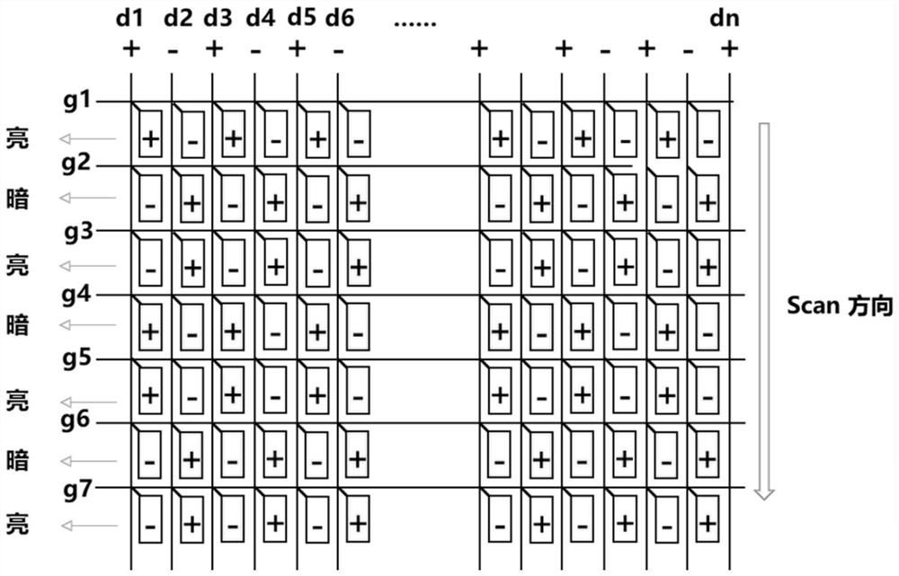
[0061] This embodiment also provides a more specific example to describe the display driving method. In the display driving method, the charging of the target pixel row is improved by taking the even-numbered pixel row as the target pixel row and then precharging the target pixel row. efficiency, reduce the brightness difference between the even-numbered pixel row and the odd-numbered pixel row, and improve the display effect, specifically:
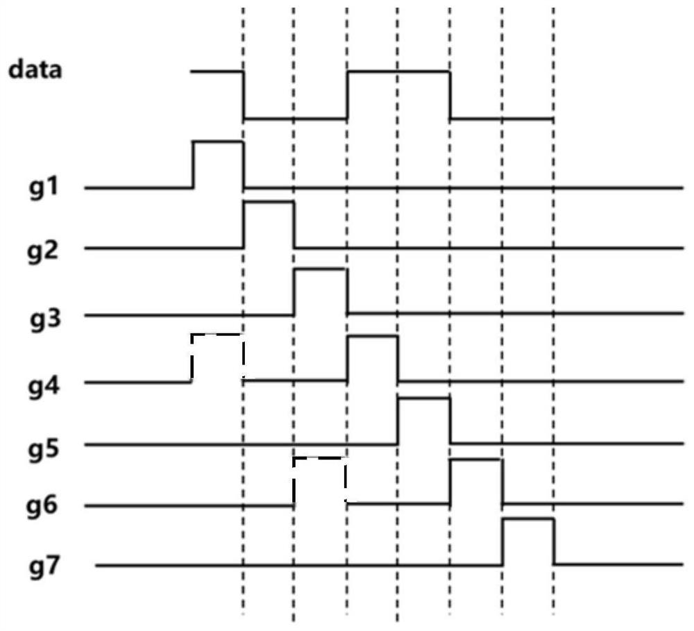
[0062] For example, as image 3 shown, image 3 It is the driving sequence diagram of the present invention, the adjacent scanning signal waveforms are different; the charging time of each row of pixels is T, for the odd row scanning lines corresponding to the odd pixel row, the scanning signal is a single square wave, and for the even row scanning lines, the scanning signal In addition to the original square wave, there is another square wave that is turned on 3T ahead of time (except the 2nd row), because the data signal, the square wa...
Embodiment 3
[0068] This embodiment also provides a more specific example to describe the display driving method. In the display driving method, the even-numbered pixel row is precharged by taking the even-numbered pixel row as the target pixel row, and then the charging of the even-numbered pixel row is improved. After the efficiency, further, the brightness of each sub-pixel of the even-numbered pixel row is increased by increasing the charging duration of the even-numbered pixel row, and / or the charging duration of the odd-numbered pixel row is reduced to reduce the brightness of each sub-pixel of the odd-numbered pixel row, thereby reducing the even-numbered pixel row. The brightness difference between the pixel row and the odd pixel row improves the uniformity of the display panel, specifically:
[0069] For example, as Figure 7 As shown, the normal scanning time width of the gate signal is H0, the width of the gate scanning signal corresponding to the pixel in the 2n+1th row is set ...
PUM
 Abstract
Description
Claims
Application Information