Semiconductor device and manufacturing method thereof
A semiconductor and device technology, applied in the field of semiconductor devices and their manufacturing, can solve difficult design and manufacturing problems
- Summary
- Abstract
- Description
- Claims
- Application Information
AI Technical Summary
Problems solved by technology
Method used
Image

Examples
example 1
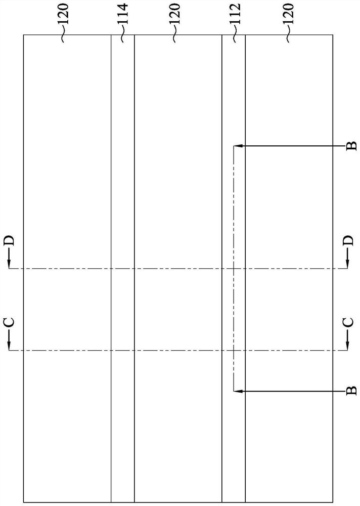
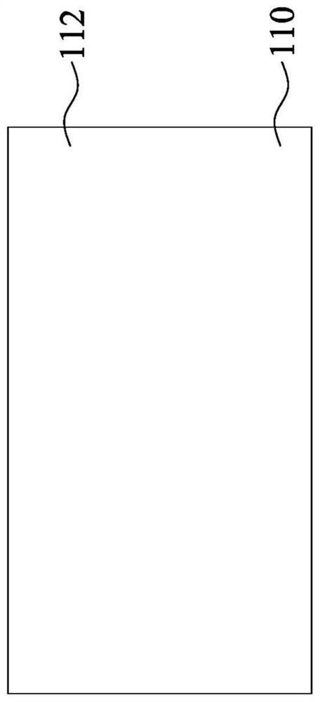
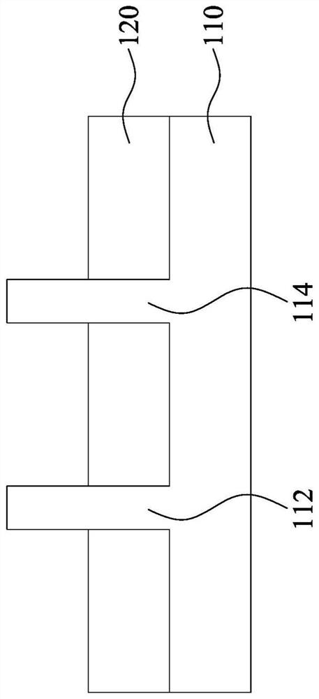
[0108] Example 1. A semiconductor device, comprising: a substrate; a first gate structure, a second gate structure and a third gate structure, the first gate structure, the second gate structure and the first gate structure A triple gate structure is located above the substrate and arranged along a first direction, wherein the first gate structure, the second gate structure and the third gate structure are different from the first direction, and the second gate structure is located between the first gate structure and the third gate structure; and a first source / drain region, the first source A pole / drain region is located between the first gate structure and the third gate structure and at one end of the second gate structure.
example 2
[0109] Example 2. The semiconductor device of example 1, wherein the first gate structure and the second gate structure have a first pitch, and the second gate structure and the third gate structure There is a second pitch that is substantially the same as the first pitch.
example 3
[0110] Example 3. The semiconductor device according to example 1, wherein the first source / drain region has a length in the first direction, and the length of the first source / drain region is greater than The distance between the first gate structure and the second gate structure.
PUM
 Abstract
Description
Claims
Application Information
PatSnap Eureka turns technology decisions into work you can execute. Powered by our Innovation Knowledge Graph, it runs expert workflows across engineering, life sciences, materials and intellectual property. Get your review-ready output in minutes.


