
Light-emitting device, display substrate and display device
A technology for light-emitting devices and light-emitting layers, which is applied in the manufacture of electric solid-state devices, semiconductor devices, and semiconductor/solid-state devices, etc., can solve problems such as color crosstalk and lateral current drift, and achieve the purpose of preventing high voltage, reducing lateral current, and ensuring Effect of device voltage and performance
- Summary
- Abstract
- Description
- Claims
- Application Information
AI Technical Summary
Problems solved by technology
Method used
Image

Examples
Embodiment Construction
[0035] The following will clearly and completely describe the technical solutions in the embodiments of the present application with reference to the drawings in the embodiments of the present application. Obviously, the described embodiments are part of the embodiments of the present application, not all of them. Based on the embodiments in this application, all other embodiments obtained by persons of ordinary skill in the art without creative efforts fall within the protection scope of this application.
[0036] The light emitting device provided by the embodiment of the present application will be described in detail below.
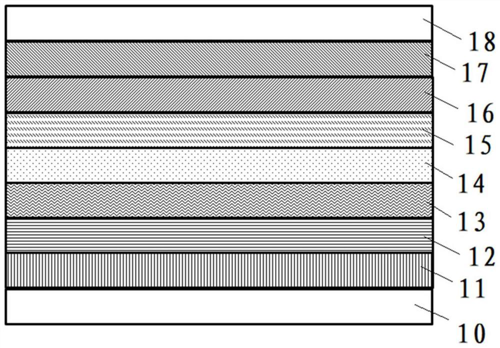
[0037] Such as figure 2 As shown, the light-emitting device of the embodiment of the present invention includes a hole injection layer 11, a hole transport layer 12, an electron blocking layer 13, a light-emitting layer 14, and an electron injection layer 17 that are sequentially stacked, wherein the light-emitting layer 14 includes a plurality of li...
PUM
| Property | Measurement | Unit |
|---|---|---|
| thickness | aaaaa | aaaaa |
Abstract
Description
Claims
Application Information