
A processing technology and processing system of a circuit fixing board

A processing technology and processing system technology, applied in the field of sheet metal parts processing, can solve the problem of low processing accuracy of circuit fixing boards, and achieve the effects of preventing dimensional changes, ensuring processing accuracy, and improving accuracy

Active Publication Date: 2022-06-03
SHENZHEN KONCOIL TECH
View PDF4 Cites 0 Cited by
  • Summary
  • Abstract
  • Description
  • Claims
  • Application Information

AI Technical Summary

Problems solved by technology

[0005] In order to improve the problem of low machining accuracy of the circuit fixing board caused by the size change around the interface fixing convex hull in the process of processing the interface fixing convex hull, the application provides a processing technology and a processing system for the circuit fixing board

Method used


Image

  • A processing technology and processing system of a circuit fixing board
  • A processing technology and processing system of a circuit fixing board
  • A processing technology and processing system of a circuit fixing board

Examples


Embodiment 1

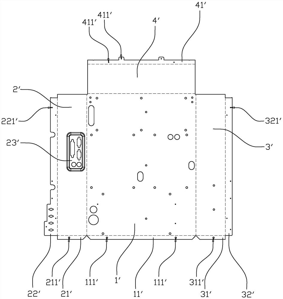
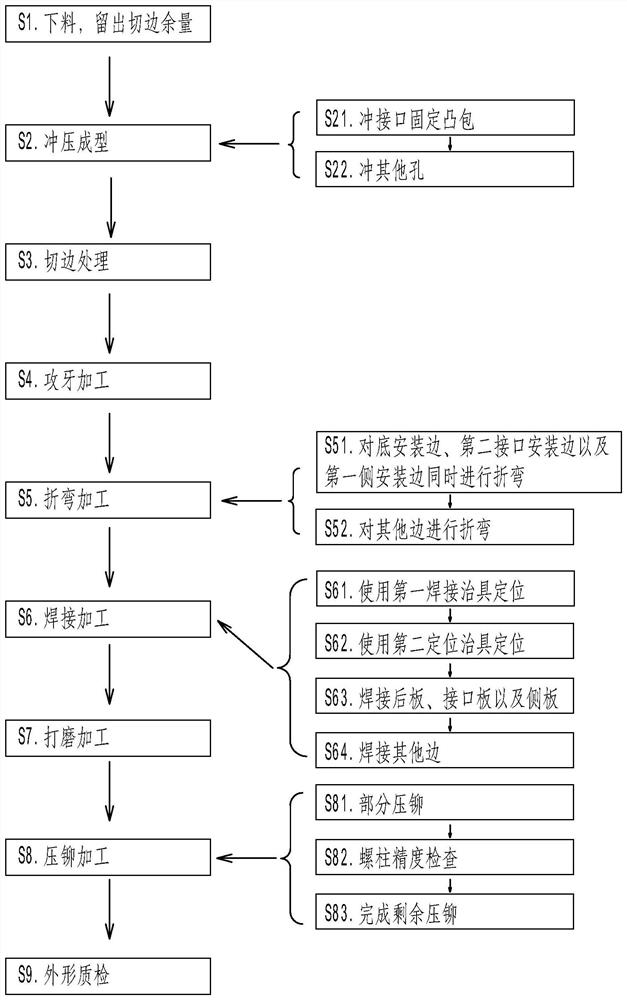
[0069] The embodiment of the present application discloses a process for processing a circuit fixing board. refer to figure 2 and image 3 , a processing technology of a circuit fixing board, comprising the following steps:

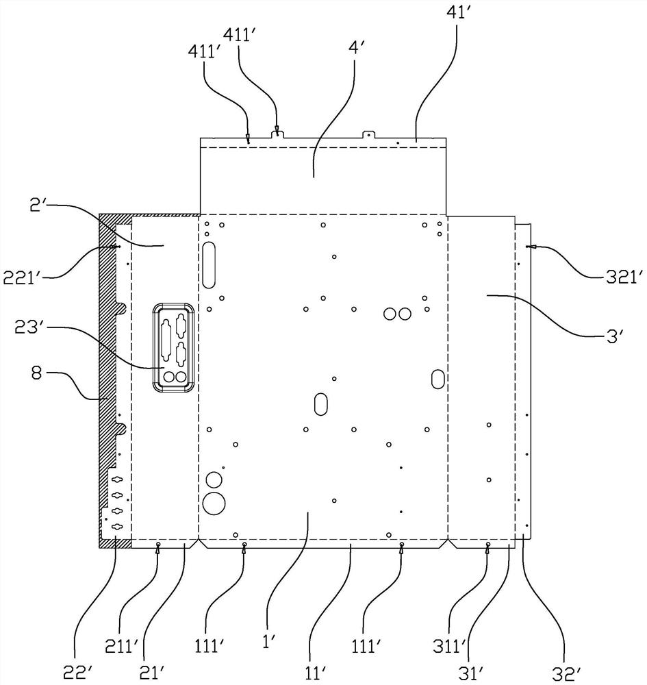
[0070] S1. Cut the whole sheet metal plate according to the unfolded size of the sheet metal, and at the same time leave a trimming allowance of 8 at the position of the second interface installation side 22'; the process of cutting the whole sheet metal plate at the blanking station, Unloading can be done on a laser cutting machine or on a number punching machine. In the first embodiment, the entire sheet metal is processed by blanking on a number punching machine according to the expanded size of the sheet metal.

[0071] S2. stamping and forming the interface board 2'; wherein, the process of stamping the interface board 2' at the general punching station can be divided into the following two steps;

[0072] S21. Use the interface convex hull die ...

Embodiment 2

[0097] The embodiment of the present application discloses a processing system for a circuit fixing board. A processing system for a circuit fixing board, comprising a blanking station for cutting a whole sheet metal plate into the shape of a part, a general punching station and a tapping station for punching out correspondingly shaped convex hulls or through holes , bending station, welding station, grinding station, pressure riveting station and quality inspection station.

[0098] The welding station includes a welding machine for welding, a first welding fixture 1 for positioning the bottom mounting edge 11', the first interface mounting edge 21' and the first side mounting edge 31', and a rear mounting edge for positioning. 41', the second interface mounting edge 22' and the second side mounting edge 32' for positioning the second soldering fixture 2, after the circuit fixing board is bent, there is a circuit fixing cavity 9, and the first soldering fixture 1 is located i...


PUM


Abstract

This application relates to the field of sheet metal parts processing, and in particular to a processing technology for circuit fixing boards, which includes the following steps: S1. While blanking the entire sheet metal board, leave a trimming edge at the position of the second interface mounting edge Surplus; S2. Stamping and forming the interface board; S3. Trimming the trimming margin; S4. Tapping the circuit fixing board; S5. Bending the circuit fixing board; S6. Perform welding processing on the circuit fixing plate; S7. Grind the welded part; S8. Perform pressure riveting processing on the holes designed with pressure riveting studs on the circuit fixing plate. By leaving a trimming margin on the side of the interface plate, the material around the stamping position has enough deformation space. The sheet metal material undergoes plastic deformation after stamping deformation, and the material will not shrink back. After the stamping process is completed Finally, the interface board is trimmed to remove the deformed material, thereby effectively controlling the dimensional accuracy of the interface board shape.

Description

technical field [0001] The present application relates to the field of sheet metal parts processing, and in particular, to a processing technology and a processing system of a circuit fixing board. Background technique [0002] In automatic control equipment, while the circuit fixing board is used as the installation basis for installing the circuit board and other electronic components, the circuit fixing board can protect the circuit board and other electronic components. The control module on the circuit board needs to be electrically connected with the corresponding action module, therefore, various data exchange interfaces are usually provided on the circuit board. In order to prevent the data exchange interface on the circuit board from being loosened from the circuit board during the process of plugging and unplugging the cable, when the circuit board is fixed on the circuit fixing board, it is necessary to set the corresponding interface fixing boss on the circuit fi...

Claims


Application Information

Patent Timeline
Patent Type & Authority Patents(China)
IPC IPC(8): B23P15/00B23P23/06
CPCB23P15/00B23P23/06
Inventor 王小锋章代红张勇厉晓明
Owner SHENZHEN KONCOIL TECH
Learn More