Light-emitting element and display device
A light-emitting element and light-emitting layer technology, which is applied in the field of display devices and light-emitting elements, can solve the problems of low grayscale reproducibility of OLED and QLED, and achieve the effect of suppressing brightness deviation
- Summary
- Abstract
- Description
- Claims
- Application Information
AI Technical Summary
Problems solved by technology
Method used
Image
Examples
no. 1 approach 〕
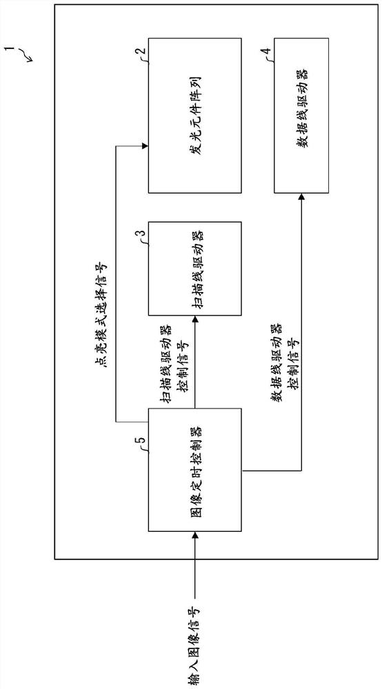
[0056] figure 1 It is a diagram showing a schematic configuration of the display device 1 according to the first embodiment.
[0057] The display device 1 includes a light-emitting element array 2 provided with light-emitting elements (not shown) on an active matrix substrate (not shown), a scan line driver (Scan driver) 3, a data line driver (Data driver) 4, and an image Timing controller 5 (circuit).
[0058] The input image signal is input to the image timing controller 5, and the lighting mode selection signal is output from the image timing controller 5 to the light emitting element array 2, and the scanning line driver control signal is output from the image timing controller 5 to the scanning line driver 3, and the image timing controller 5 outputs the scanning line driver control signal from the image timing controller 5. The timing controller 5 outputs a data line driver control signal to the data line driver 4 .
[0059] The scan line driver 3 switches the require...
no. 2 approach 〕
[0123] Below, based on Figure 11 to Figure 16 A second embodiment of the present invention will be described. The light-emitting elements included in the light-emitting element arrays 32 and 52 of this embodiment are different from the first embodiment in that the area of the first region L1 and the area of the fourth region L4 are different from those of the first embodiment. described in . For convenience of description, members having the same functions as those shown in the drawings of the first embodiment are given the same reference numerals, and description thereof will be omitted.
[0124] Figure 11 It is a diagram showing a schematic configuration of the light emitting element array 32 . In addition, in Figure 11 In the drawing, only one light emitting element provided on the active matrix substrate 19 which is a part of the light emitting element array 32 including a plurality of light emitting elements is shown.
[0125] Figure 12 (a) is a top view of ...
PUM
 Abstract
Description
Claims
Application Information


