
Light-emitting apparatus, backlight unit, liquid crystal display apparatus, and illumination apparatus

A technology for light-emitting devices and backlight units, which is applied to optics, electrical components, nonlinear optics, etc., can solve the problems of brightness deviation and chromaticity deviation of light-emitting devices, and achieves suppression of brightness deviation, chromaticity deviation, and reduction of graininess. Effect

Active Publication Date: 2016-02-03
PANASONIC CORP
View PDF9 Cites 0 Cited by
  • Summary
  • Abstract
  • Description
  • Claims
  • Application Information

AI Technical Summary

Problems solved by technology

[0011] However, the problem of the SMD-type light-emitting device is that it becomes a non-light-emitting area between adjacent SMD-type LED elements, so that when the light is turned on, the appearance is grainy, and brightness variation occurs. chromaticity deviation

Method used


Image

  • Light-emitting apparatus, backlight unit, liquid crystal display apparatus, and illumination apparatus
  • Light-emitting apparatus, backlight unit, liquid crystal display apparatus, and illumination apparatus
  • Light-emitting apparatus, backlight unit, liquid crystal display apparatus, and illumination apparatus

Examples


Embodiment 1

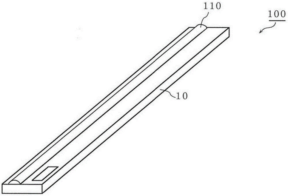
[0068] First, for the schematic structure of the light-emitting device 100 according to Embodiment 1 of the present invention, use figure 1 Be explained. figure 1 It is an overview perspective view of the light-emitting device according to Embodiment 1 of the present invention.

[0069] Such as figure 1 As shown, the light emitting device 100 according to Embodiment 1 of the present invention is a linear light source that emits light in a linear shape (line shape), and includes a light emitting unit 110 that is formed linearly on the substrate 10 and emits predetermined light. As will be described later, the light emitting unit 110 is composed of a plurality of LED chips arranged in a line (one-dimensionally) and a sealing member containing a phosphor.

[0070] Furthermore, the light emitting device 100 according to this embodiment is a COB type (Chip On Board) light emitting device in which an LED chip (bare chip) directly mounted on the substrate 10 is sealed with a pho...

Embodiment 2

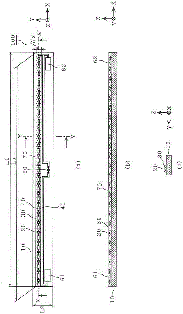
[0140] Next, for the light-emitting device 200 according to the second embodiment of the present invention, using Figure 9 Be explained. Figure 9 (a) is a plan view of a light emitting device according to Example 2 of the present invention. and, Figure 9 (b) is a cross-sectional view of the light-emitting device according to Example 2 of the present invention (substrate longitudinal cross-section) cut along the XX' line of (a), Figure 9 (c) is a cross-sectional view of the light-emitting device according to Example 2 of the present invention cut along the YY' line of (a) (cross-section in the short direction of the substrate).

[0141] The structure of the light emitting device 200 according to the second embodiment of the present invention is basically the same as that of the light emitting device 100 according to the first embodiment of the present invention. The light emitting device 200 according to the present embodiment differs from the light emitting device 100 a...

Embodiment 3

[0171] Hereinafter, application examples of the light-emitting device according to Embodiments 1 and 2 of the present invention will be described based on Embodiments 3 to 5. FIG.

[0172] First, for an example in which the light-emitting device according to Embodiments 1 and 2 of the present invention is applied to a backlight unit for a liquid crystal display device, use Figure 13 Be explained. Figure 13 It is an exploded perspective view of the backlight unit according to Embodiment 3 of the present invention.

[0173] Such as Figure 13 As shown, the backlight unit 300 according to Embodiment 3 of the present invention is an edge-light type backlight unit in which a light source is arranged on the side of a light guide plate, and includes a housing 310, a reflective sheet 320, a light guide plate 330, a light emitting device 340, an optical Thin plate group 350, and front frame 360.

[0174] The housing 310 has a flat box shape and is formed by pressing a steel plate ...


PUM


Abstract

A light-emitting apparatus (100) according to the present invention includes: an elongated substrate (10); a plurality of LEDs (20) arranged in a straight line on the substrate (10) in a longitudinal direction of the substrate (10); and a sealing member (30) that includes an optical wavelength converter and seals the LEDs (20), wherein the sealing member (30) is formed in a straight line in a direction of arrangement of the LEDs (20) and seals the LEDs (20) collectively.

Description

[0001] The present invention is a divisional application of patent application 201280018773.1 submitted on October 16, 2013, and the entire content of the parent application is cited here. technical field [0002] The present invention relates to a light-emitting device, a backlight unit, a liquid crystal display device, and a lighting device, and particularly to a light-emitting device using a semiconductor light-emitting element. Background technique [0003] In recent years, semiconductor light emitting elements such as light emitting diodes (LED: Light Emitting Diode) are high-efficiency and space-saving light sources, so they are used as backlight light sources in liquid crystal display devices such as liquid crystal televisions, or as light sources for illumination in lighting devices. etc. are widely used. [0004] In the backlight light source and the light source for illumination, LEDs are unitized as a light emitting device (light emitting module). [0005] Conven...

Claims


Application Information

Patent Timeline
Patent Type & Authority Applications(China)
IPC IPC(8): H01L33/50H01L33/54H01L25/075H01L25/16
CPCH01L25/0753H01L33/52H01L33/54H01L33/50H01L25/167H01L2224/48091H01L2933/005H01L2924/00014G02F1/133615H01L27/153H01L33/507H01L33/62H01L2933/0016H01L2933/0041H01L2933/0066
Inventor 杉浦健二
Owner PANASONIC CORP
Learn More