

OLED display device
A display device and display panel technology, applied in the direction of identification devices, instruments, etc., can solve the problems of large arc shape in the bending area, abnormality, film fracture display in the bending area, etc.
- Summary
- Abstract
- Description
- Claims
- Application Information
AI Technical Summary
Problems solved by technology
Method used
Image

Examples
Embodiment Construction
[0019] The following will clearly and completely describe the technical solutions in the embodiments of the present invention with reference to the drawings in the embodiments of the present invention. In the drawings, for clarity and ease of understanding and description, the size and thickness of the components shown in the drawings are not in scale.
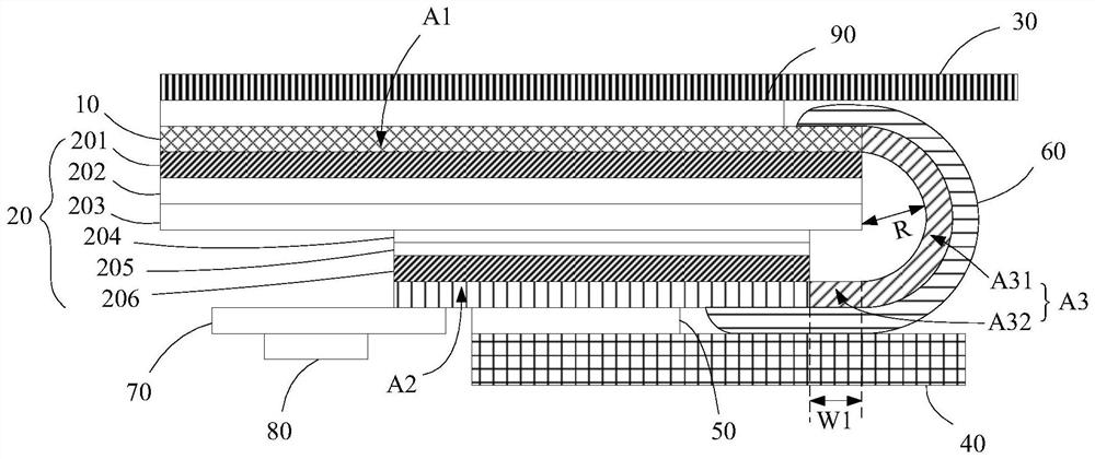
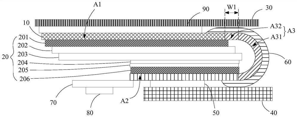
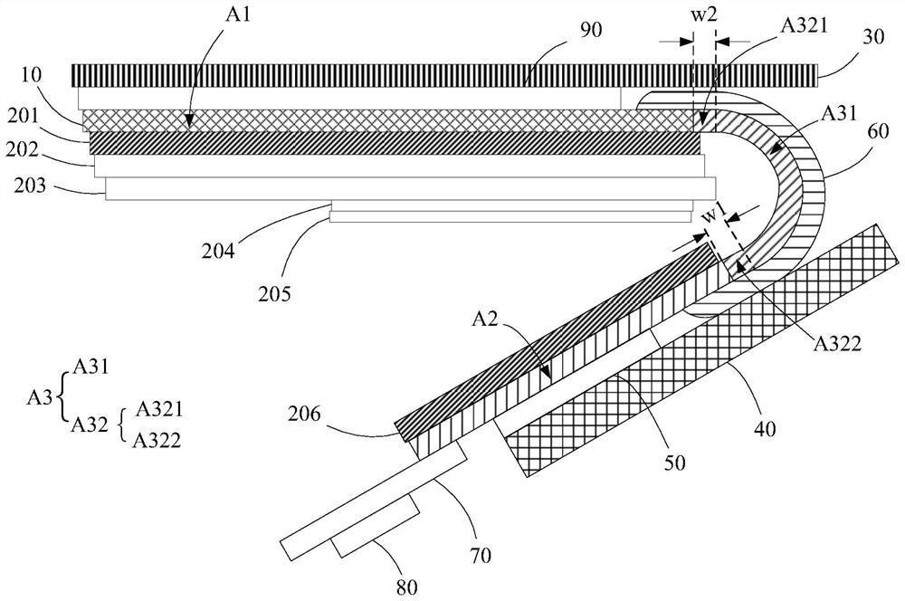
[0020] Such as figure 1 As shown, it is a schematic diagram of the basic structure of an OLED display device provided by an embodiment of the present invention. The OLED display device includes an OLED display panel 10, a support assembly 20, and a cover plate 30. The OLED display panel 10 includes a first planar area A1, The second plane area A2 and the bending area A3 connecting the first plane area A1 and the second plane area A2, the bending area A3 includes an arcuate area A31 and a slip transition area A32; the support assembly The two sides of 20 are attached to the backlight side of the OLED display panel 10 in the fi...
PUM
| Property | Measurement | Unit |
|---|---|---|
| length | aaaaa | aaaaa |
| radius | aaaaa | aaaaa |
Abstract
Description
Claims
Application Information