Mechanical support within molded chip package
A packaging and chip mounting technology, applied in electrical components, electrical solid-state devices, semiconductor devices, etc., to solve problems such as contact space occupied
- Summary
- Abstract
- Description
- Claims
- Application Information
AI Technical Summary
Problems solved by technology
Method used
Image
Examples
Embodiment Construction
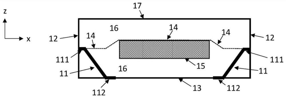
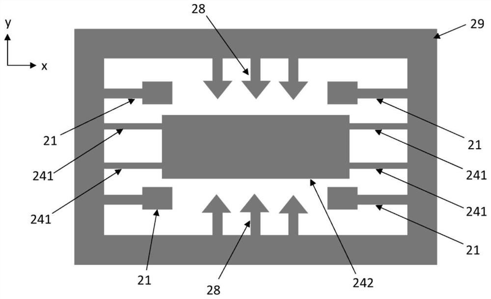
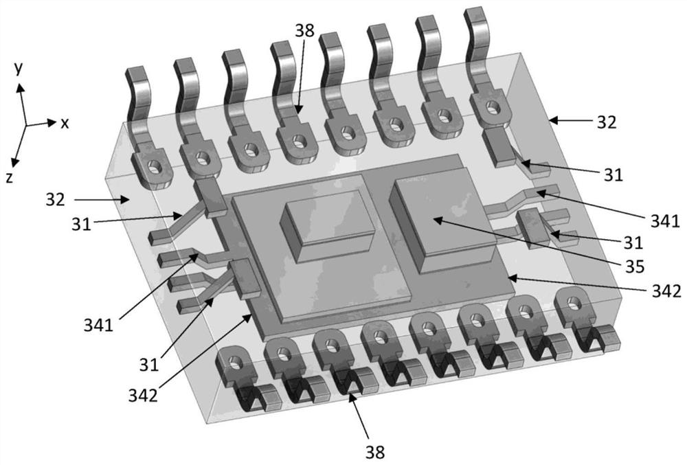
[0018] The present disclosure describes an electronic component that includes a package body that includes a set of side walls and a bottom wall that shares a common edge with each of the set of side walls. The bottom and side walls define an enclosed interior space, and each side and bottom wall have an inner surface and an outer surface. One or more chip mounting elements extend from the inner surface of the at least one side wall into the enclosed interior space. At least one electronic chip is attached to the one or more chip mounting elements within the enclosed interior space. The electronic component also includes one or more stiffening elements extending from the inner surface of one of the side walls to the outer surface of the bottom wall within the enclosed interior space. The one or more stiffening elements are separated from the one or more chip mounting elements within the enclosed interior space.
[0019] The chip mounting elements may include support elements...
PUM
 Abstract
Description
Claims
Application Information


