
Structure for solving splicing height difference between single modules by post-processing PCB (Printed Circuit Board) substrate

A height difference and substrate technology, applied in the field of RGB direct display, can solve the problem of uneven height of PCB substrate

Pending Publication Date: 2022-06-28
江西兆驰晶显有限公司
View PDF0 Cites 0 Cited by
  • Summary
  • Abstract
  • Description
  • Claims
  • Application Information

AI Technical Summary

Problems solved by technology

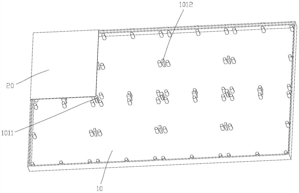
[0005] Aiming at the deficiencies of the prior art, the present invention provides a post-processing PCB substrate to solve the splicing height difference structure between a single module and a single module, aiming to solve the technical problem of unevenness of the PCB substrate installed on the base in the prior art

Method used


Image

  • Structure for solving splicing height difference between single modules by post-processing PCB (Printed Circuit Board) substrate
  • Structure for solving splicing height difference between single modules by post-processing PCB (Printed Circuit Board) substrate
  • Structure for solving splicing height difference between single modules by post-processing PCB (Printed Circuit Board) substrate

Examples


Embodiment Construction

[0029] The technical solutions in the embodiments of the present invention will be clearly and completely described below with reference to the accompanying drawings in the embodiments of the present invention. Obviously, the described embodiments are part of the embodiments of the present invention, but not all of the embodiments. Based on the embodiments of the present invention, all other embodiments obtained by those of ordinary skill in the art without creative efforts shall fall within the protection scope of the present invention.

[0030] In the description of the invention, it should be understood that the terms "center", "lateral", "top", "bottom", "left", "right", "vertical", "horizontal", "top", " The orientation or positional relationship indicated by "bottom", "inside", "outside", etc. is based on the orientation or positional relationship shown in the accompanying drawings, and is only for the convenience of describing the present invention and simplifying the de...


PUM


Abstract

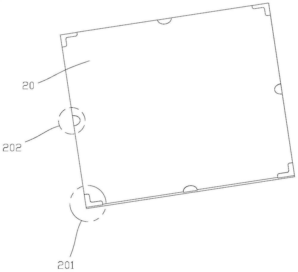
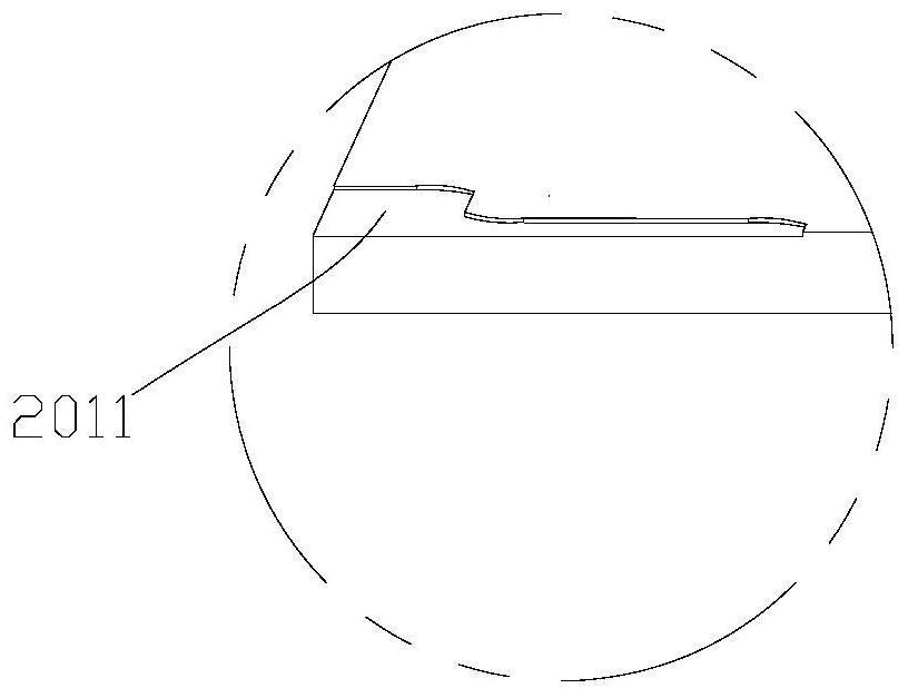
The embodiment of the invention discloses a post-processing PCB (Printed Circuit Board) substrate structure for solving the splicing height difference between single modules, which comprises a plurality of PCB substrates, and first step structures are formed at four corners of each PCB substrate; the bottom plate is provided with a supporting part, the supporting part is arranged between the PCB substrate and the bottom plate, and meanwhile, the end face, bearing the PCB substrate, of the supporting part is parallel to the first lower step of the first step structure; wherein the first lower steps of the first step structures are located on the same horizontal plane, and the supporting parts are in contact with the first lower steps of the first step structures, so that the PCB substrate is borne by the bottom plate, the technical problem that the height difference occurs when a plurality of PCB substrates are spliced due to the fact that the height difference of supplied materials of the PCB substrates is not easy to control is solved, and the quality of the PCB substrates is improved. And the phenomena that bright and dark lines appear at the side view angle of the Mini LED product and light leakage appears at the front view angle are eliminated.

Description

technical field [0001] The invention relates to the technical field of RGB direct display, in particular to a post-processing PCB substrate to solve the splicing height difference structure of a single module and a single module. Background technique [0002] Mini LED is the most mature LED screen display technology after small spacing. It not only has the characteristics of small spacing LED seamless splicing, wide color gamut, low power and long life, but also has better protection and higher information. . [0003] Usually Mini LED products are assembled from multiple PCB substrates, and the light-emitting surfaces of Mini LED products are all smooth surfaces, so that the flatness of the light-emitting surface of Mini LED products formed by splicing multiple PCB substrates is relatively high. [0004] At present, the PCB substrate and the bottom plate in the industry usually use magnets or screws to fix the PCB substrate and the bottom plate directly. At the same time, t...

Claims


Application Information

Patent Timeline
IPC IPC(8): G09F9/33H05K1/02
CPCG09F9/33H05K1/02
Inventor 江伟芳游锋吴钊剑何胜斌
Owner 江西兆驰晶显有限公司
Learn More