Fin FET devices from bulk semiconductor and method for forming

A semiconductor, fin-like technology, applied in the field of manufacturing fin field effect transistors, can solve the problem of not providing a method to control the height of the fin

Inactive Publication Date: 2007-01-24
GLOBALFOUNDRIES INC
View PDF3 Cites 6 Cited by
  • Summary
  • Abstract
  • Description
  • Claims
  • Application Information

AI Technical Summary

Problems solved by technology

[0008] Also, Hisamoto's process does not provide a way to control fin height

Method used


Image

  • Fin FET devices from bulk semiconductor and method for forming
  • Fin FET devices from bulk semiconductor and method for forming
  • Fin FET devices from bulk semiconductor and method for forming

Examples


Embodiment Construction

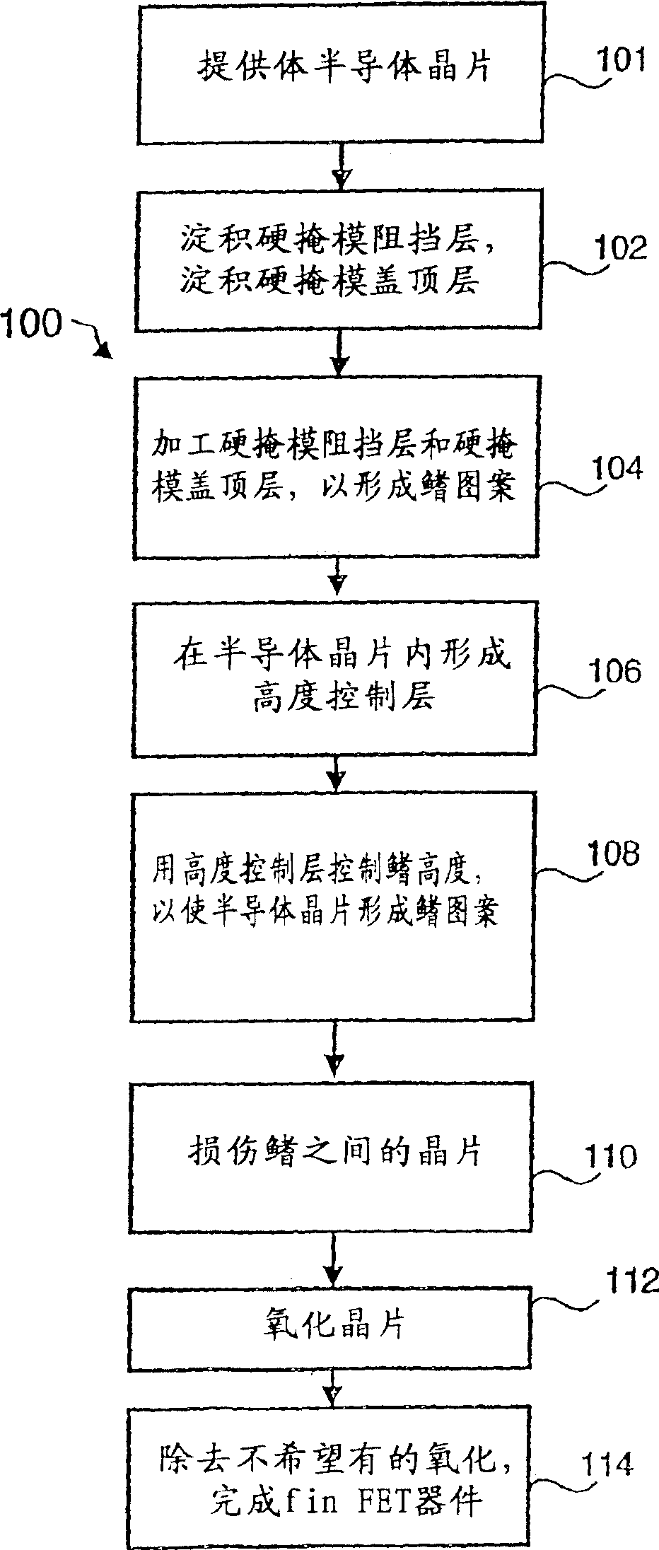
[0018] Accordingly, the present invention provides a device structure and method for forming a Fin Field Effect Transistor (FET) that overcomes many of the disadvantages of the prior art. Specifically, the device structure and method enable formation of finFET devices from bulk semiconductor wafers while improving device uniformity. This approach facilitates the formation of finFET devices from bulk semiconductor wafers and provides improved control over fin height. In addition, this approach enables the formation of finFETs from bulk semiconductors while providing isolation between individual fins and between the source and drain regions of individual finFETs. Finally, this approach can also provide optimization of the fin width. The device structure and method of the present invention therefore has the advantage that uniform finFETs can be fabricated on bulk wafers.

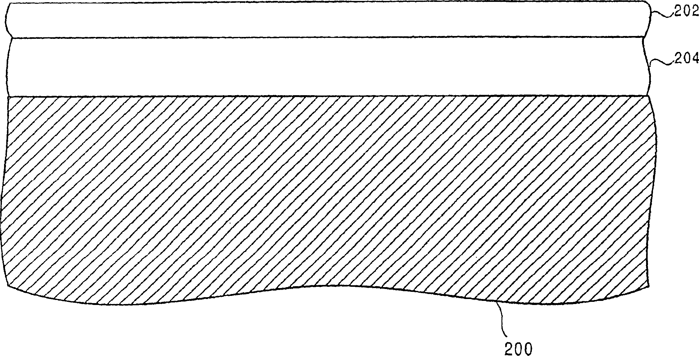
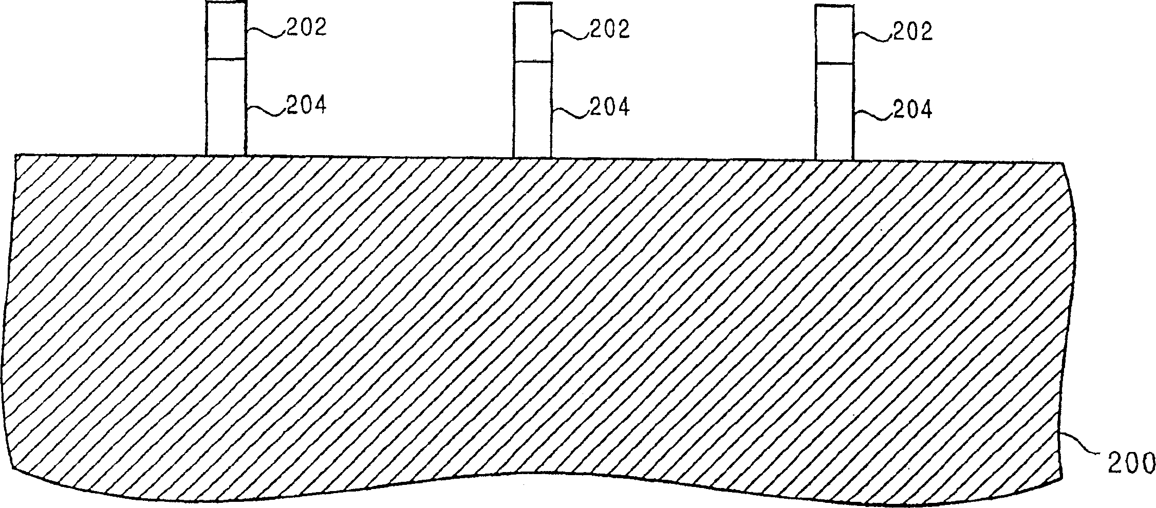
[0019] One embodiment of the present invention uses a process prior to fin patterning to provide improved ...


PUM


Abstract

The present invention thus provides a device structure and method for forming fin Field Effect Transistors (FETs) that overcomes many of the disadvantages of the prior art. Specifically, the device structure and method provides the ability to form finFET devices from bulk semiconductor wafers while providing improved wafer to wafer device uniformity. Specifically, the method facilitates the formation of finFET devices from bulk semiconductor wafers with improved fin height control. Additionally, the method provides the ability to form finFETs from bulk semiconductor while providing isolation between fins and between the source and drain region of individual finFETs. Finally, the method can also provide for the optimization of fin width. The device structure and methods of the present invention thus provide the advantages of uniform finFET fabrication while using cost effect bulk wafers.

Description

technical field [0001] The present invention relates to the field of semiconductor fabrication and, in particular, to methods of fabricating fin field effect transistors. Background technique [0002] Competing demands to reduce cost and increase performance in the production of semi-devices are driving ever-increasing device densities within integrated circuits. In order to increase device density, there is a constant need for new techniques to reduce the physical size of these semiconductor devices. [0003] The need to increase device density is particularly strong in CMOS technologies such as the design and fabrication of field effect transistors (FETs). FETs include the main components of CMOS. Scaling FETs to achieve higher device densities in CMOS can result in reduced performance and / or reliability. [0004] One type of FET that has been proposed to facilitate increased device density is the fin field effect transistor (fin Field Effect Transistor). In a finFET, ...

Claims


Application Information

Patent Timeline
Patent Type & Authority Patents(China)
IPC IPC(8): H01L21/8232H01L27/088H01L21/265H01L21/336H01L21/8234H01L21/8238H01L29/78H01L29/786
CPCH01L29/7853H01L29/7851H01L21/823828H01L29/66818H01L29/66795H01L29/785
Inventor 戴维·M.·弗雷德爱德华·J.·诺瓦克贝思·安·雷尼德温得拉·K.·萨达纳
Owner GLOBALFOUNDRIES INC
Why Eureka
Try Eureka