Complementary metal oxide semiconductor output circuit

A technology of oxide semiconductor and output circuit, which is applied in the direction of semiconductor devices, circuits, logic circuit connection/interface layout, etc.

Inactive Publication Date: 2002-11-06
SEIKO INSTR INC
View PDF0 Cites 0 Cited by
  • Summary
  • Abstract
  • Description
  • Claims
  • Application Information

AI Technical Summary

Problems solved by technology

However, to enable the selection of each output state, the circuit must be changed and a separate manufacturing process used

Method used


Image

  • Complementary metal oxide semiconductor output circuit
  • Complementary metal oxide semiconductor output circuit
  • Complementary metal oxide semiconductor output circuit

Examples


Embodiment Construction

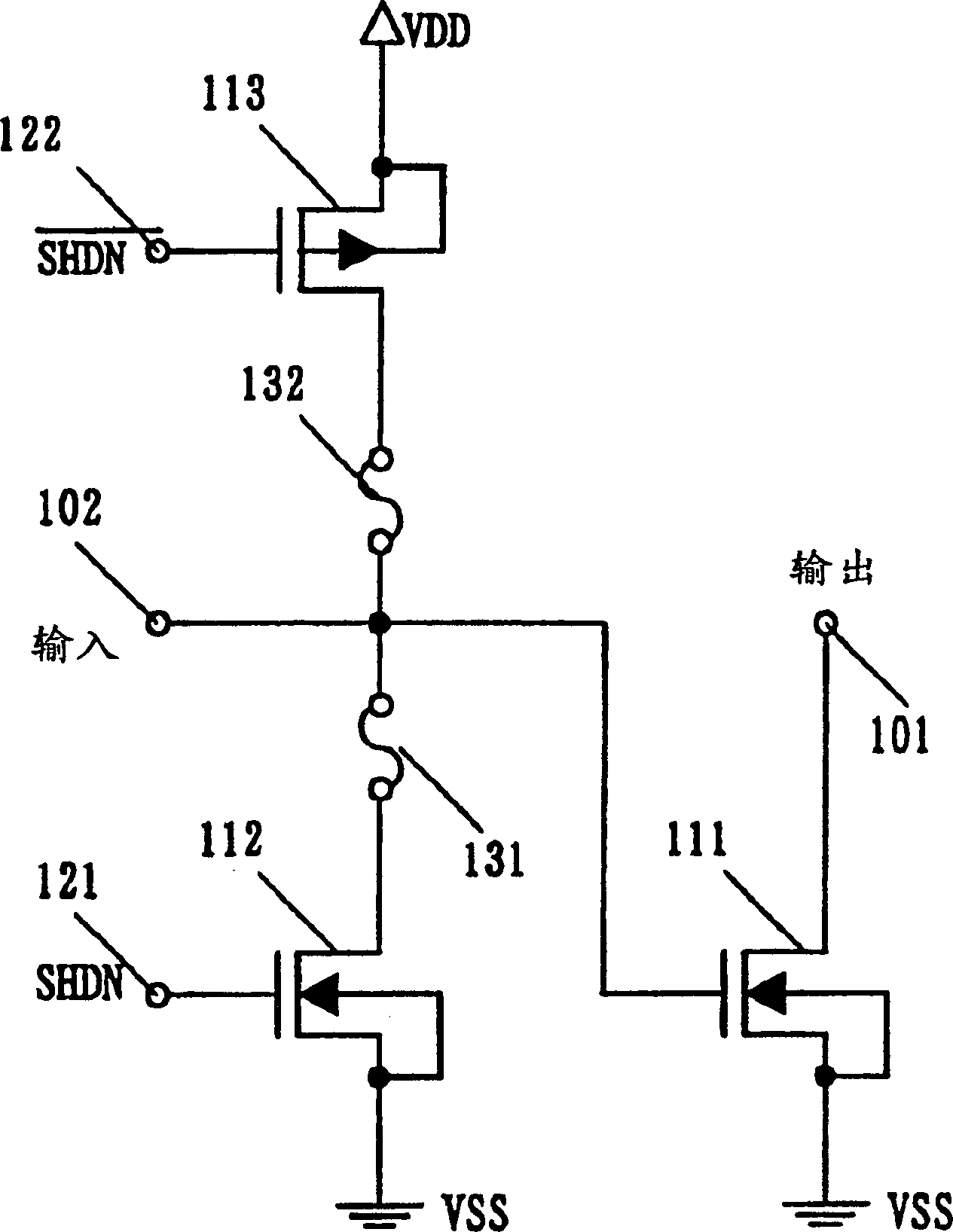
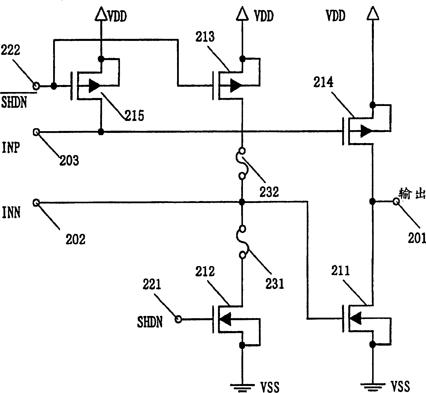
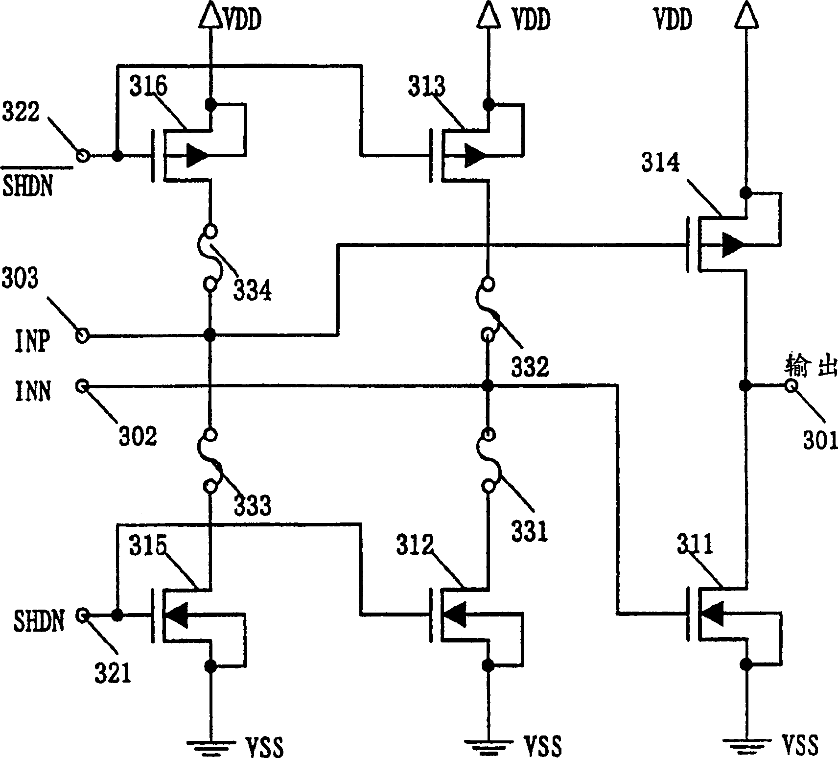
[0013] The embodiments of the present invention will now be described with reference to the drawings. figure 1 , 2 , 3, 5, and 6 are schematic diagrams showing examples of CMOS output circuits according to the present invention.

[0014] Refer to figure 1 , The input terminal 102 is connected to the gate of the NMOS transistor 111. The potential of the output terminal 101 is determined by the potential of the input terminal 102. When a signal is input to the off terminals 121 and 122, the NMOS transistor 112 and the PMOS transistor 113 are turned on. If the fuse 132 is disconnected and the fuse 131 is conductive at this time, the gate potential of the NMOS transistor 111 is pulled to VSS, so that the NMOS transistor 111 is turned off, thereby setting a high impedance at the output terminal 101. Conversely, if the fuse 131 is disconnected and the fuse 132 is conductive, the gate potential of the NMOS transistor 111 is pulled to VDD, the NMOS transistor 111 is turned on, and the p...


PUM


Abstract

A circuit that selects the output when it is off by some means. The switching element is connected between the gate of a certain transistor in the output stage and a terminal having a potential of VDD level or VSS level so as to select the gate potential.

Description

Technical field [0001] The present invention relates to a complementary metal oxide semiconductor (CMOS) circuit used to determine the output when it is turned off. technical background [0002] Figure 4 shows an example of a conventional CMOS output circuit. The operation of the conventional CMOS output circuit will now be described with reference to FIG. 4. The gate terminal of the PMOS (P-channel metal oxide semiconductor) transistor 414 is connected to the input terminal 403, and the gate terminal of the NMOS (N-channel metal oxide semiconductor) transistor 411 is connected to the input terminal 402. The voltage of the output terminal 401 is determined by the operating current of the PMOS transistor 414 and the NMOS transistor 411. When the off signal 422 is input to the gate of the PMOS transistor 413, the PMOS transistor 413 is turned on, pulling the potential at the terminal 403 to VDD, so that the PMOS transistor 414 is turned off. Similarly, the input of the shutdown sig...

Claims


Application Information

Patent Timeline
IPC IPC(8): H03K19/0175G11C7/10
CPCG11C7/1051G11C7/1057
Inventor 木村亮平
Owner SEIKO INSTR INC
Why Eureka
Try Eureka