Method of measuring built crystal layer thickness
An epitaxial layer, epitaxial technology, applied in the direction of measurement devices, semiconductor/solid-state device testing/measurement, instruments, etc.
- Summary
- Abstract
- Description
- Claims
- Application Information
AI Technical Summary
Problems solved by technology
Method used
Image

Examples
Embodiment Construction
[0015] It should be noted here that the process steps and structures described below do not include a complete process. The present invention can be implemented by means of various integrated circuit process technologies, and only those process technologies required for an understanding of the present invention are mentioned here.
[0016] Hereinafter, the present invention will be described in detail according to the accompanying drawings. Please note that the drawings are in simple form and not drawn to scale, and the dimensions are exaggerated to facilitate understanding of the present invention.
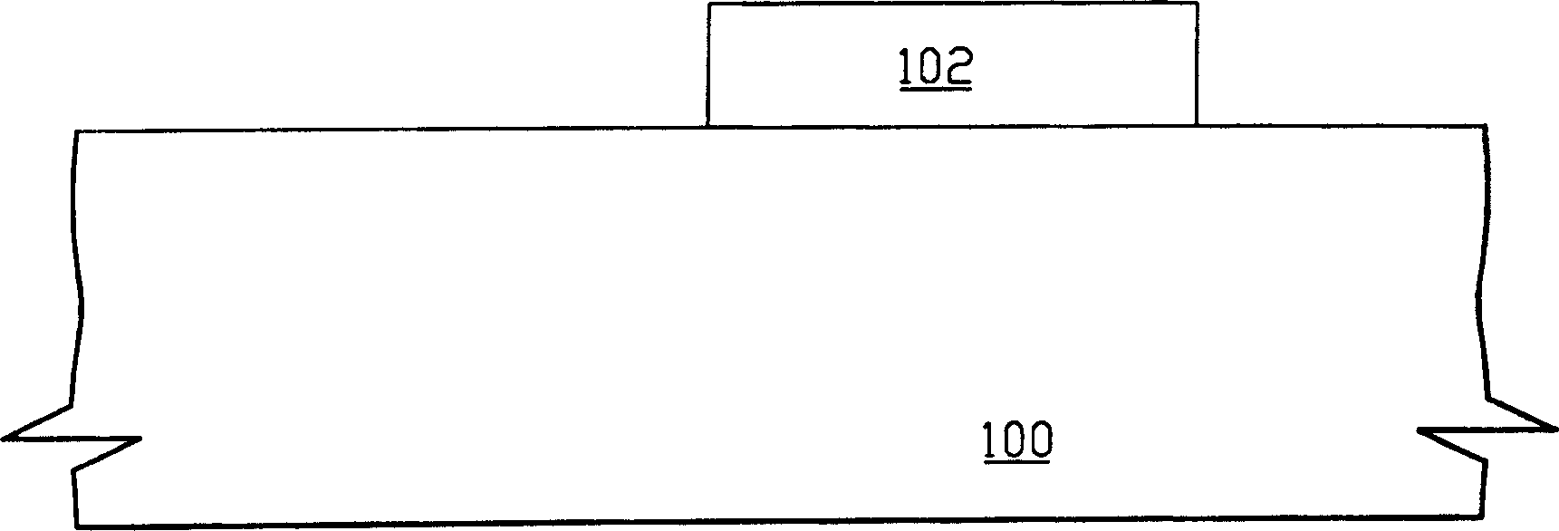
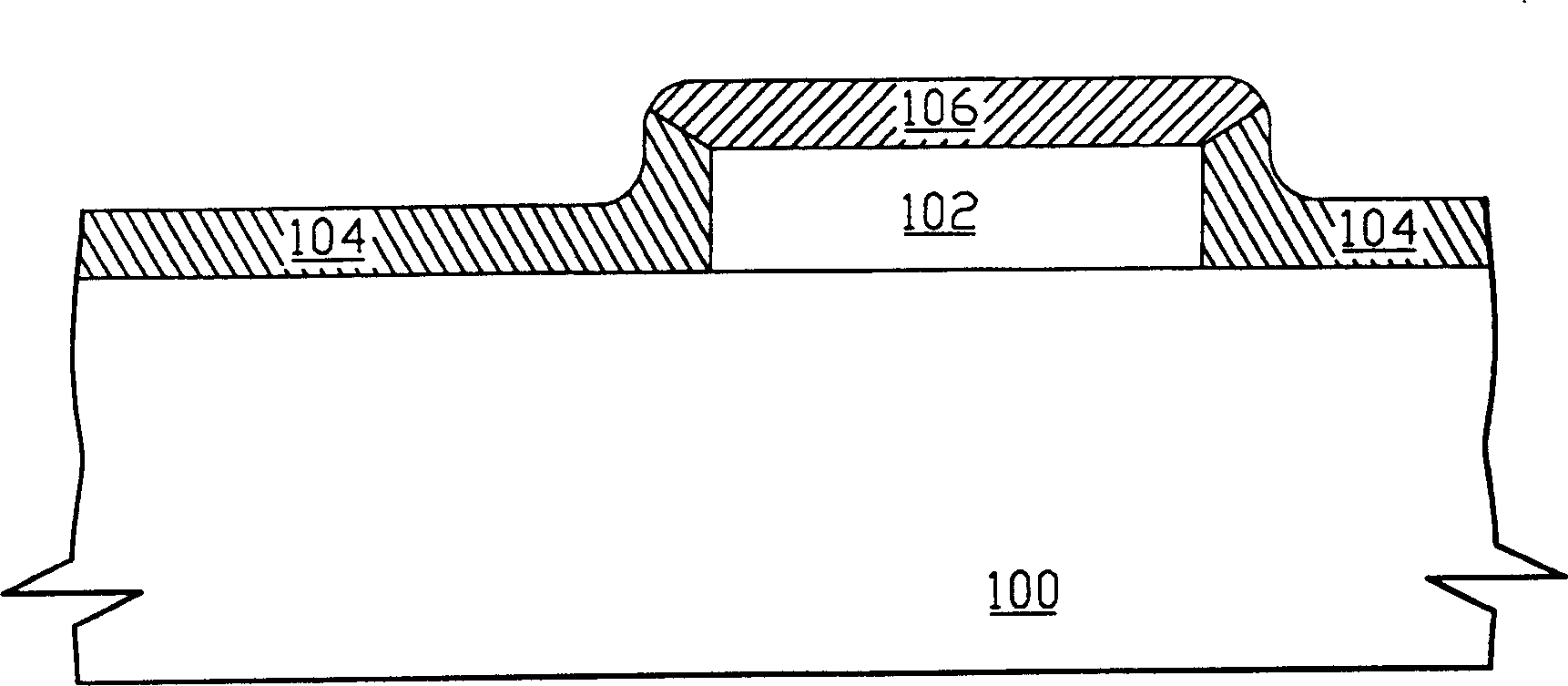
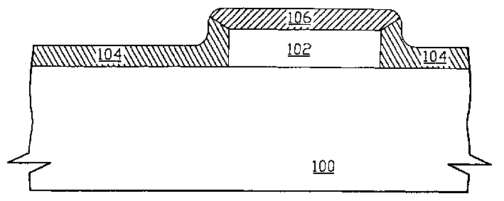
[0017] refer to figure 1 As shown, a substrate 100 is shown having a layer 102 thereon. The substrate 100 includes at least a semiconductor substrate, such as a silicon substrate with a lattice orientation, but not limited to a silicon substrate with a lattice orientation. The substrate 100 may also include other semiconductor substrates such as diamond-like carbon, and may a...
PUM
 Abstract
Description
Claims
Application Information