Pinned photodiode structure and method of formation

Active Publication Date: 2005-01-06
APTINA IMAGING CORP
View PDF12 Cites 55 Cited by
  • Summary
  • Abstract
  • Description
  • Claims
  • Application Information

AI Technical Summary

Benefits of technology

[0027] In one aspect, the invention provides a pinned photodiode for an imager cell and a method of forming the photodiode with a shallow pinned surface layer near an adjacent transistor gate. The shallow pinned surface layer with sub-regions of varying dopant concentrations can be further improved using dual surface implants of varying strength. The pinned surface layer is first formed with an angled implant from a

Problems solved by technology

Currently, there are a number of common problems associated with conventionally formed photodiodes, such as the pinned photodiode 11 of FIG. 2.
However, the barrier at the transfer gate's edge 30 still blocked complete charge transfer and photographic images still suffered from low-light image lag.
Moreover, diffusion of both doped p+ region 4 and n-type region 35 remained, which is undesirable.
As a result, the current flow is not completely controlled by the transfer gate 30.
Another problem associated with the conventional pinned photodiode 11 of FIG. 3 is charge capacity loss and variation from sensor to sensor.
This mutual compensation results in photosensor performance variation.
The mutual diffusion and implant straggle result in an uncontrolled implant region at the transfer gate's edge 30 that gives rise to barrier and lag issues.
An incomplete transfer of charge results in image lag.

Method used


Image

  • Pinned photodiode structure and method of formation
  • Pinned photodiode structure and method of formation
  • Pinned photodiode structure and method of formation

Examples


Embodiment Construction

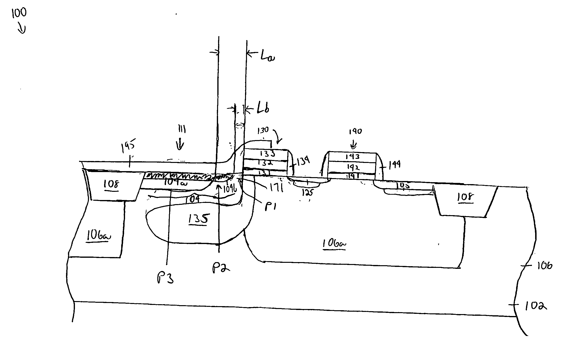
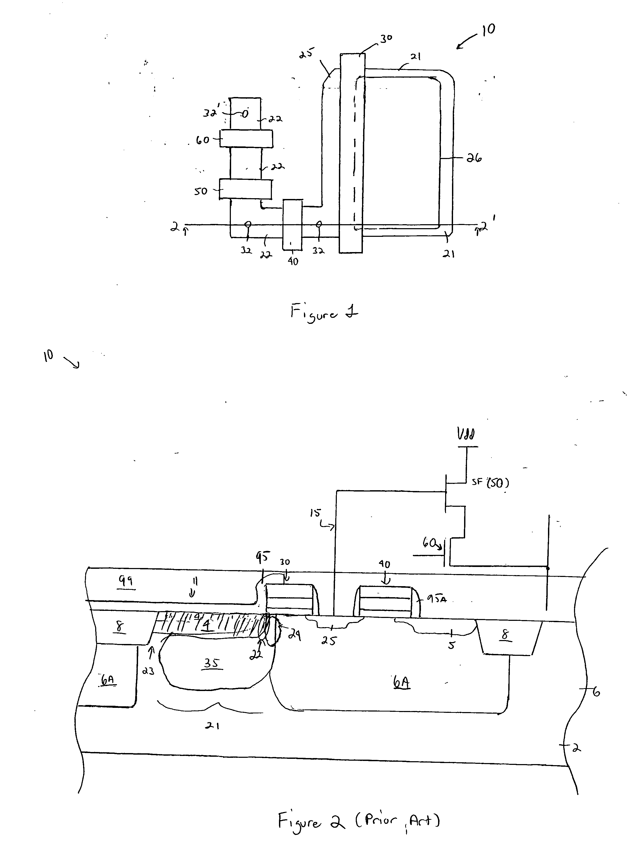
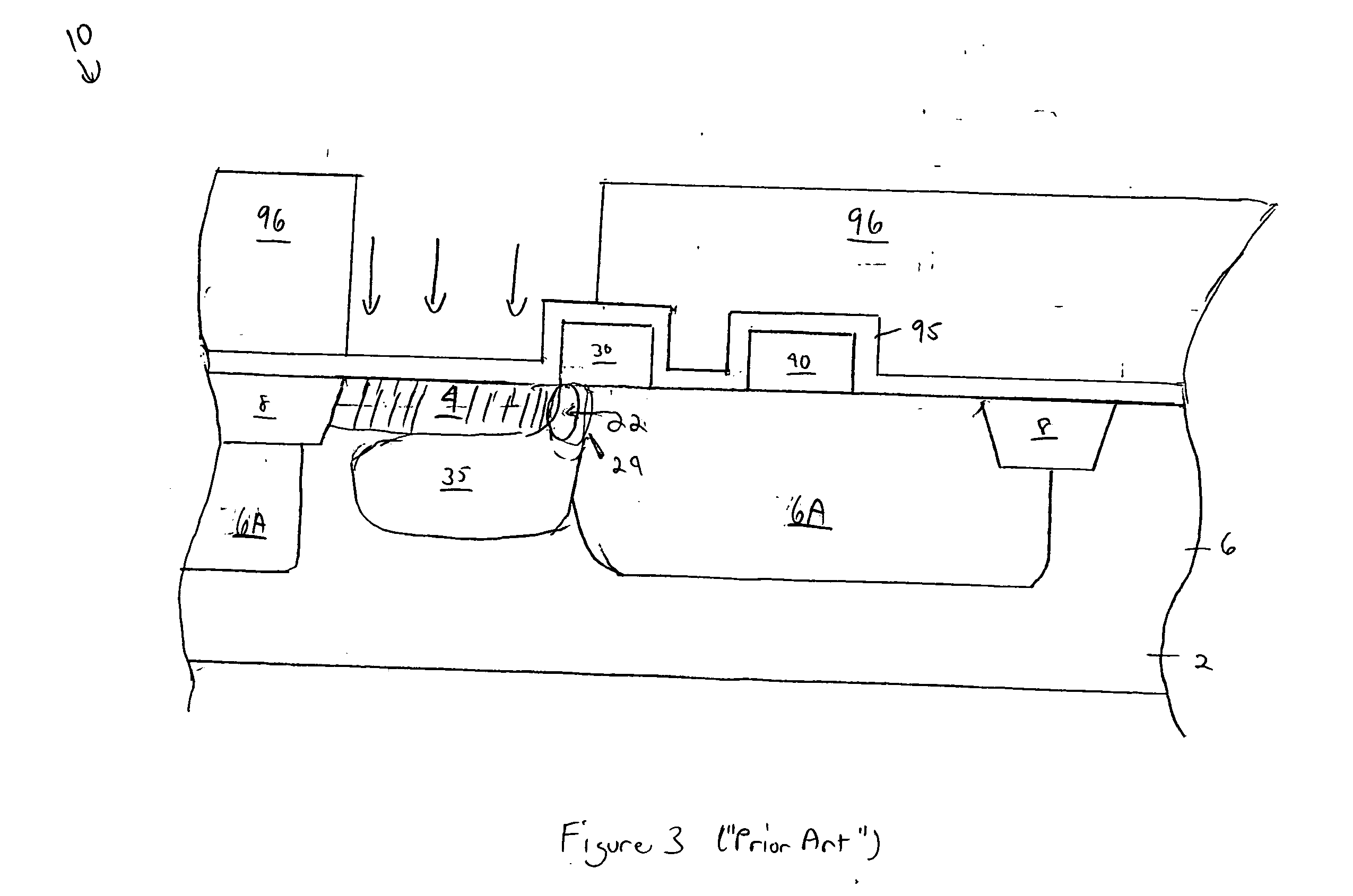
[0040] In the following detailed description, reference is made to the accompanying drawings which form a part hereof, and in which is shown by way of illustration specific embodiments in which the invention may be practiced. These embodiments are described in sufficient detail to enable those skilled in the art to practice the invention, and it is to be understood that other embodiments may be utilized, and that structural, logical and electrical changes may be made without departing from the spirit and scope of the present invention.

[0041] The terms “wafer” and “substrate” are to be understood as a semiconductor-based material including silicon, silicon-on-insulator (SOI) or silicon-on-sapphire (SOS) technology, doped and undoped silicon semiconductors, epitaxial layers of silicon supported by a base semiconductor foundation, and other semiconductor structures.

[0042] Furthermore, when reference is made to a “wafer” or “substrate” in the following description, previous process st...


PUM


Abstract

An imager having a photodiode with a shallow doping profile with respect to the top surface of a substrate is disclosed. An imager with a graded pinned surface layer, self-aligned to a gate stack is provided. A photodiode with a shallow doping profile with respect to the top surface of a substrate and a graded pinned surface layer, self-aligned to a gate stack is provided. These photodiodes exhibit reduced image lag, transfer gate leakage, and photodiode dark current generation.

Description

CROSS REFERENCE TO RELATED APPLICATION [0001] This non-provisional application claims the benefit of provisional application Serial No.: 60 / 483,895, filed Jul. 2, 2003, which is hereby incorporated by reference.FIELD OF THE INVENTION [0002] The present invention relates to the field of semiconductor devices and, in particular, to a pinned photodiode used in an imaging device and a method of forming the pinned photodiode. BACKGROUND OF THE INVENTION [0003] The semiconductor industry currently uses different types of semiconductor-based imagers, including charge coupled devices (CCD) and CMOS imager devices. Because of the inherent limitations in CCD technology, CMOS imagers have been increasingly used as low-cost imaging devices. [0004] A CMOS image sensor circuit includes a focal plane array of pixel cells, each one of the cells including a photoconversion device, for example, a photogate, photoconductor, or a photodiode for accumulating photogenerated charge in a doped portion of t...

Claims


Application Information

Patent Timeline
IPC IPC(8): H01L27/146H01L27/148H01L31/062
CPCH01L27/14603H01L27/1463H01L27/14812H01L27/14656H01L27/14689H01L27/14643
Inventor RHODES, HOWARD E.
Owner APTINA IMAGING CORP
Why Eureka
Try Eureka