Voltage controlled oscillator with wide frequency band

A voltage-controlled oscillator, wide-band technology, applied in power oscillators, electrical components, etc., can solve the problems of different output signal amplitudes, phase noise fluctuations, etc.

Active Publication Date: 2005-05-11
PEKING UNIV +1
View PDF0 Cites 2 Cited by
  • Summary
  • Abstract
  • Description
  • Claims
  • Application Information

AI Technical Summary

Problems solved by technology

[0019] (1) Due to the large range of ω variation, the start-up conditions of the voltage-controlled oscillator are significantly different at different frequency points, that is, the required g mn or g mp There is a significant difference
(2) Due to the large range of ω variation, the amplitude of the output signal is significantly different at different frequency points, so the phase noise also fluctuates greatly

Method used


Image

  • Voltage controlled oscillator with wide frequency band
  • Voltage controlled oscillator with wide frequency band
  • Voltage controlled oscillator with wide frequency band

Examples


Embodiment Construction

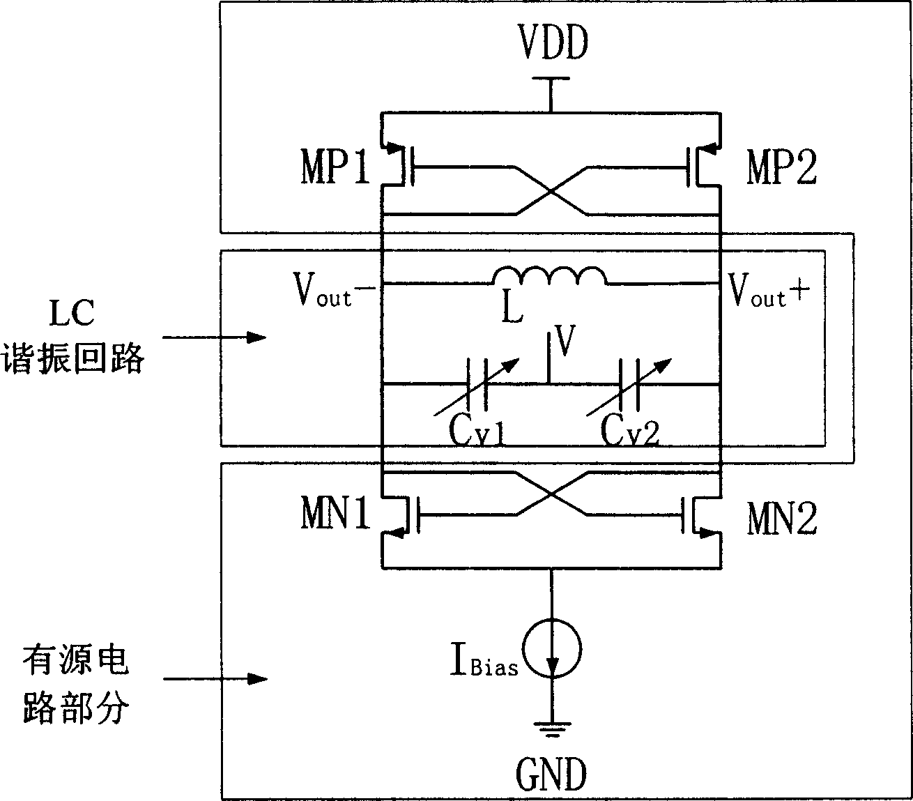
[0030] Such as Figure 4 As shown, the present invention is implemented in a typical VCO circuit (such as figure 1 It is improved on the basis of shown). and figure 1 compared to, Figure 4 Another negative conductance circuit is added to the . That is, a total of two negative conductance circuit networks are controlled by respective switches. When both negative conductance circuits are connected, it is equivalent to changing the size of the MOS device in the active circuit (that is, w and l in formulas (3) and (4)) and the bias current I of the entire circuit Bias (i.e. I Bias =I Rias1 +I Bias2 ). It can be known from formulas (3) and (4) that the present invention essentially changes g by changing the size of the MOS device or the current flowing through the MOS device mn and g mp value. When the required negative conductance is large (eg low frequency band), both negative conductance circuit networks can be connected at the same time; when the required negative c...


PUM


Abstract

The invention consists of LC resonance loop used in providing negative conductance active device. The current of the above negative conductance circuit is tunable. The invention uses variable negative conductance circuit structure by which multi negative conductance circuit network can link and cut off. By varying the total equivalent negative conductance the variable negative conductance circuit can optimally neutralize the conductance loss to meet the condition of oscillation of oscillator and make phase noise and amplitude of output signal to reach optimal value.

Description

technical field [0001] The invention relates to a radio frequency voltage-controlled oscillator, in particular to a wide-band voltage-controlled oscillator. Background technique [0002] In the past ten years, personal wireless communication systems such as pagers, cordless phones, analog and digital cellular phones, as well as digital TV and broadcasting have developed rapidly, and wireless communication has become the most important industry after the PC industry. Due to the characteristics of small size, low power consumption and low cost of integrated circuits, the vigorous development of wireless communication technology has contributed to the rapid development of radio frequency integrated circuits. At present, radio frequency integrated circuits have become one of the important research fields of microelectronics. Designing and researching high-performance key circuit modules has become a vital driving force for the advancement of radio frequency integrated circuit t...

Claims


Application Information

Patent Timeline
Patent Type & Authority Applications(China)
IPC IPC(8): H03B5/12
Inventor 石浩张国艳廖怀林黄如张兴王阳元
Owner PEKING UNIV
Why Eureka
Try Eureka