Semiconductor packaging and semiconductor module
A semiconductor and electrical conductivity technology, applied in the field of semiconductor modules, can solve the problems of increased plane size, large semiconductor package, unfavorable equipment investment and engineering management, etc., to achieve the effect of miniaturization
- Summary
- Abstract
- Description
- Claims
- Application Information
AI Technical Summary
Problems solved by technology
Method used
Image

Examples
Example
[0037] (First embodiment)
[0038] Reference Figure 1 to Figure 6 The first embodiment of the present invention will be described.
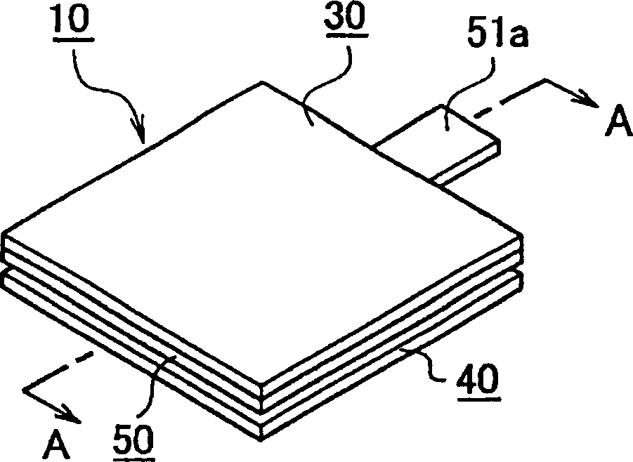
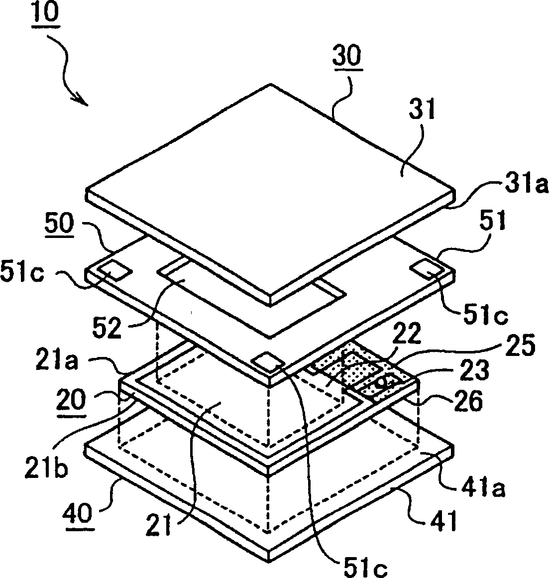
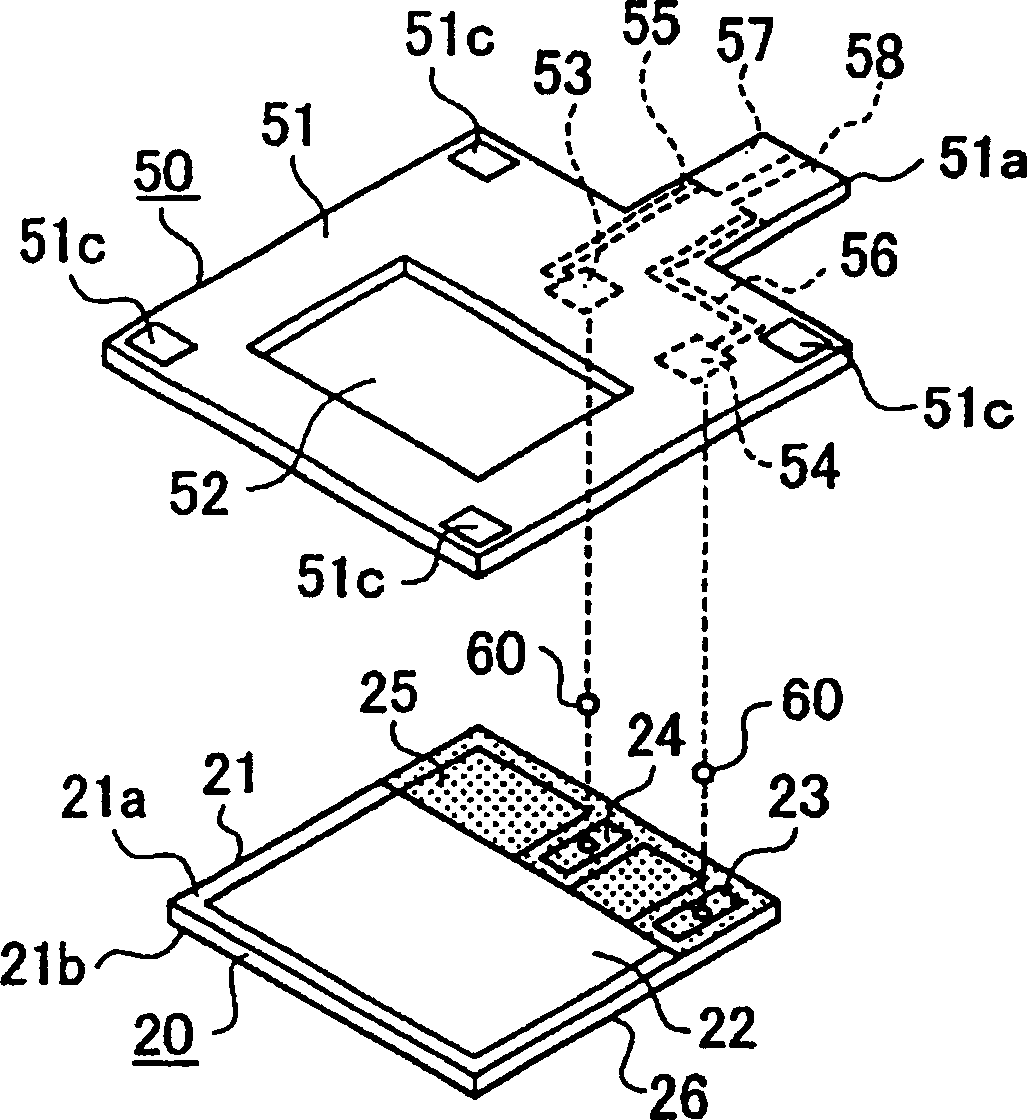
[0039] Such as figure 1 with figure 2 As shown, the semiconductor package 10 is constituted by laminating the following components: an IGBT element (semiconductor element) 20 as a power semiconductor element; a first electrode plate 30 arranged on the surface (main surface) 21a side of the IGBT element 20; The second electrode plate 40 on the side of the back surface 21 b that faces the surface of the IGBT element 20; the insulating substrate 50 arranged between the first electrode plate 30 and the IGBT element 20. The outer peripheral edge of the IGBT element 20 is provided inside the outer peripheral edges of the first electrode plate 30, the second electrode plate 40, and the insulating substrate 50.
[0040] IGBT element 20 such as figure 2 with image 3 As shown, the IGBT is mounted on a so-called semiconductor chip 21 which is a small plate...
Example
[0064] (Second embodiment)
[0065] Refer to Figure 7 to Figure 9 The second embodiment of the present invention will be described.
[0066] The second embodiment of the present invention is basically the same as the first embodiment, and in the second embodiment, parts different from the first embodiment will be described. In addition, in the second embodiment, the same parts as those described in the first embodiment are denoted by the same reference numerals, and the description thereof is omitted (the same applies to the other embodiments).
[0067] The difference between the second embodiment and the first embodiment is as follows:Figure 7 As shown, the opposing surface (first power electrode) 31a of the first electrode plate 30 on the IGBT element 20 side becomes a plane, the IGBT element 20 and the first electrode plate 30 are soldered together, and the IGBT element 20 and the insulating substrate 50 are soldered together. The welding and the brazing of the IGBT element 20...
Example
[0077] (Third Embodiment)
[0078] Refer to Picture 10 The third embodiment of the present invention will be described.
[0079] The third embodiment of the present invention is basically the same as the second embodiment, and the parts of the third embodiment that are different from the second embodiment will be described.
[0080] The difference between the third embodiment and the second embodiment is as follows: Picture 10 As shown, in the semiconductor package 10, a resin portion 80 is provided between the first electrode plate 30 and the second electrode plate 40, which surrounds the IGBT element 20.
[0081] By filling the space between the first electrode plate 30 and the second electrode plate 40 with resin, the resin portion 80 is provided around the IGBT element 20. As a result, the first electrode plate 30 and the second electrode plate 40 are fixed to each other, and the periphery of the IGBT element 20 is covered by the resin portion 80.
[0082] In this way, accor...
PUM
 Abstract
Description
Claims
Application Information
 - R&D Engineer
- R&D Manager
- IP Professional
- Industry Leading Data Capabilities
- Powerful AI technology
- Patent DNA Extraction
Browse by: Latest US Patents, China's latest patents, Technical Efficacy Thesaurus, Application Domain, Technology Topic.
© 2024 PatSnap. All rights reserved.Legal|Privacy policy|Modern Slavery Act Transparency Statement|Sitemap