Method of manufacturing a semiconductor device

A technology of semiconductors and amorphous semiconductors, which is applied in semiconductor devices, semiconductor/solid-state device manufacturing, electrical components, etc., and can solve problems such as high leakage currents

Inactive Publication Date: 2006-11-01
INFINEON TECH AG
View PDF1 Cites 2 Cited by
  • Summary
  • Abstract
  • Description
  • Claims
  • Application Information

AI Technical Summary

Problems solved by technology

[0005] Disadvantageously, semiconductor devices using the above gate stack have high leakage current from the gate stack into the substrate

Method used


Image

  • Method of manufacturing a semiconductor device
  • Method of manufacturing a semiconductor device
  • Method of manufacturing a semiconductor device

Examples


Embodiment Construction

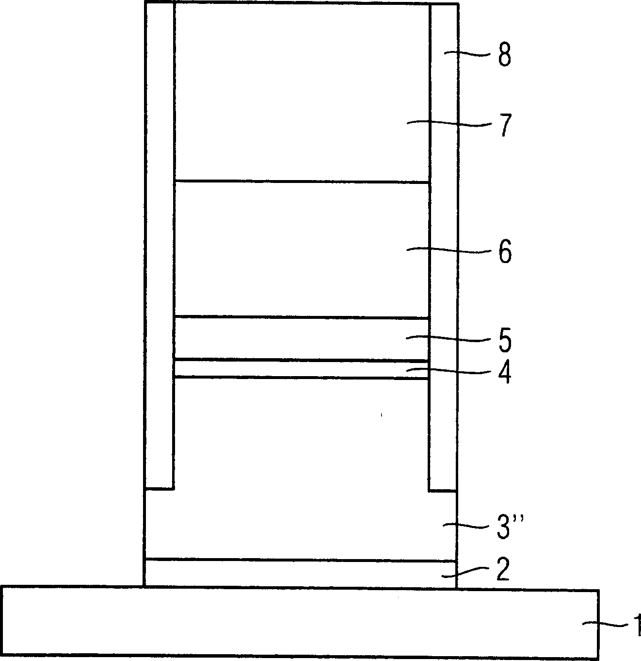
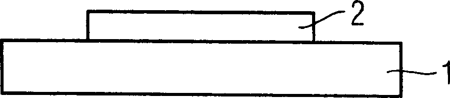
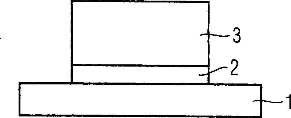
[0041] figure 1 A partial cross-sectional view of the gate stack is shown. On the substrate 1, a vertical gate stack is placed with the layers starting with the layer closest to the substrate 1 in the following order: gate dielectric layer 2, doped polycrystalline semiconductor layer 3", some intermediate layers 4, 5. Form the metal layer 6 of the contact or wire and the final cap layer nitride 7. The nitride or oxide spacer (spacer) 8 can be vertically arranged in the stack along all layers except the gate dielectric layer 2 at the side.

[0042] Substrate 1 contains a typical semiconductor structure, including drain and source regions arranged in different ways ( figure 1 not shown). Typically, the substrate 1 is positively (p-type) or negatively (n-type) doped.

[0043] A dielectric layer 2 is provided on the substrate above the gate region placed between the drain region and the source region. This dielectric layer 2 forms a gate dielectric layer isolating the subst...


PUM

PropertyMeasurementUnit
thicknessaaaaaaaaaa

Abstract

The invention relates to a method of manufacturing a semiconductor device, in which a substrate is provided, a dielectric layer is formed on top of the substrate, an amorphous semiconductor layer id deposited on top of the dielectric layer, the amorphous semiconductor layer is doped, and a high temperature step to the amorphous layer is applied to form a crystallized layer out of the amorphous semiconductor.

Description

technical field [0001] The present invention relates to a method of manufacturing a semiconductor device and a semiconductor device manufactured by the method. Background technique [0002] Although the invention can in principle be applied to any desired integrated circuit, the invention and its potential problems will hereafter be described with reference to a gate stack. [0003] Active semiconductor structures with field effect transistors are widely used in electrical circuits. The necessary gate structure is typically provided with a vertical gate stack over the gate channel in the substrate 51, such as image 3 shown. The gate stack comprises, in the following order, an isolation layer 52 forming a gate dielectric layer; a heavily doped semiconductor layer 53 for applying an electric field within the substrate 1 to the underlying gate channel through the gate dielectric layer; Intermediate layers 54, 55 to prevent diffusion and provide a good adhesion interface for ...

Claims


Application Information

Patent Timeline
Patent Type & Authority Applications(China)
IPC IPC(8): H01L21/20H01L21/28H01L21/336H01L29/43H01L29/78
CPCH01L21/265H01L21/28044H01L21/324H01L29/4925H01L21/02667
Inventor 奥拉夫·斯托贝克延斯·哈恩斯文·施米德鲍尔于尔根·福卢弗兰克·雅库博斯基托马斯·舒斯特
Owner INFINEON TECH AG
Why Eureka
Try Eureka