Device with programmable scan chain for use in multi-chip assembly and programming method therefor

A scanning chain and chip technology, applied in special data processing applications, static memory, digital circuit testing, etc., can solve the problems of untestable scan chains, increased testing costs, and inability to obtain coverage, etc.

Active Publication Date: 2007-07-11
PROLIFIC TECH INC
View PDF1 Cites 10 Cited by
  • Summary
  • Abstract
  • Description
  • Claims
  • Application Information

AI Technical Summary

Problems solved by technology

However, although each chip of the multi-chip module has a scanning input / output port, it cannot be bonded out because of the inter-connection between the chips, so that the existing scanning Chains cannot be tested in the component phase, leading to problems with poor test coverage
In response to such problems, some additional functional tests are added to compensate for the aforementioned poor test coverage, but this increases the cost of testing and often fails to achieve the expected coverage

Method used


Image

  • Device with programmable scan chain for use in multi-chip assembly and programming method therefor
  • Device with programmable scan chain for use in multi-chip assembly and programming method therefor
  • Device with programmable scan chain for use in multi-chip assembly and programming method therefor

Examples


Embodiment Construction

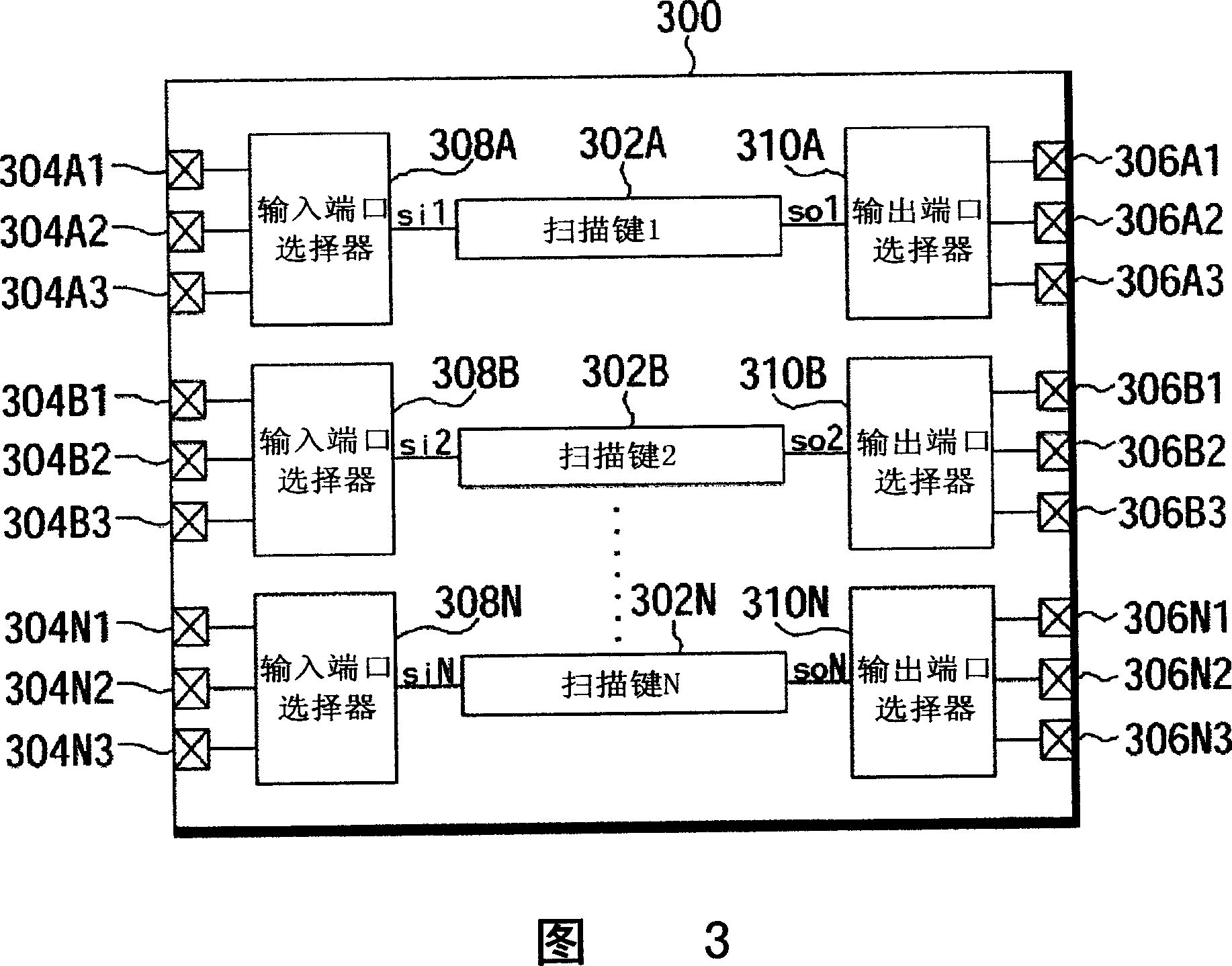
[0019] Please refer to FIG. 3 , which is a block diagram of a device with programmable scan chains according to a preferred embodiment of the present invention. Wherein, reference numeral 300 represents a chip, reference numerals 302A, 302B, . 304B2, 304B3 represent scan input ports corresponding to the scan chain 302B, and reference numerals 304N1, 304N2, 304N3 represent scan input ports corresponding to the scan chain 302N. In addition, symbols 306A1, 306A2, 306A3 represent scan output ports (scan output ports) corresponding to the scan chain 302A, symbols 306B1, 306B2, 306B3 represent scan output ports (scan output ports) corresponding to the scan chain 302B, and symbols 306N1, 306N2, 306N3 represents scan output ports corresponding to the scan chain 302N. In short, in this embodiment, three scan input ports correspond to one scan chain, and three scan output ports correspond to one scan chain. However, it only means that multiple scan input ports and multiple scan output ...


PUM


Abstract

The planning scanning chain device comprises a scanning chain with scanning input and output, several No. 1 input or output, input selector, selecting one of the input or output, coupling with the scanning input, several No. 2 input and output end, an output selector, selecting one of the No. 2 output or input with coupled scanning output. The planning scanning chain device comprises a scanning chain with scanning input and output, several No. 1 input or output, input selector, selecting one of the input or output, coupling with the scanning input, several No. 2 input and output end, an output selector, selecting one of the No. 2 output or input with coupled scanning output.

Description

technical field [0001] The present invention relates to the technology of flexible programmable scan chains applied to integrated circuit design, in particular, to a device with programmable scan chains (Programmable Scan Chains) applied to multi-chip modules and a programming method thereof. Background technique [0002] In the field of application-specific integrated circuit (Application-Specific Integrated Circuit) design, especially the integrated circuit design with a number of up to millions of transistor elements (gate-count), in order to facilitate mass production efficiency, it usually supports design for test (Design for Test) , which can be referred to as the DFT function for short. Please refer to FIG. 1 , which shows a block diagram of a chip with DFT function. Reference numeral 100 represents a chip, reference numerals 102A, 102B, ..., 102N represent scan chains, and reference numerals 104A, 104B, ..., 104N represent scan chains. Input ports (scan input ports)...

Claims


Application Information

Patent Timeline
Patent Type & Authority Applications(China)
IPC IPC(8): G01R31/317G06F17/50G11C29/54
Inventor 陈柏源詹澄胜林慧敏
Owner PROLIFIC TECH INC
Why Eureka
Try Eureka