Organic light emitting diode pixel arrangement structure and display panel

a technology of light-emitting diodes and arrangement structures, which is applied in the direction of basic electric elements, electrical equipment, semiconductor devices, etc., can solve the problems of increasing the difficulty of fmm production, the production of oled displays with high quality and high resolution still faces many challenges, etc., and achieves the effect of solving low resolution and high resolution

Active Publication Date: 2019-12-10
WUHAN CHINA STAR OPTOELECTRONICS SEMICON DISPLAY TECH CO LTD
View PDF13 Cites 1 Cited by
  • Summary
  • Abstract
  • Description
  • Claims
  • Application Information

AI Technical Summary

Benefits of technology

[0008]An object of the present disclosure is to provide an organic light emitting diode pixel arrangement structure with high resolution and a display panel so as to solve low resolution existing in existing OLED display panel.
[0029]Compared with existing organic light emitting diode pixel array structure and display panel, sub-pixels arrangement of the display panel of the embodiment of the present disclosure can simultaneously manufacture a plurality of sub-pixels using a same fine metal mask, so as to provide the display panel with high resolution and solve low resolution existing in existing OLED display panel.

Problems solved by technology

At present, people have higher and higher requirements for exquisiteness of display; however, production of OLED displays with high quality and high resolution still faces many challenges.
With an increase of resolution requirements, production of the FMM is becoming more and more difficult.

Method used


Image

  • Organic light emitting diode pixel arrangement structure and display panel
  • Organic light emitting diode pixel arrangement structure and display panel
  • Organic light emitting diode pixel arrangement structure and display panel

Examples


first embodiment

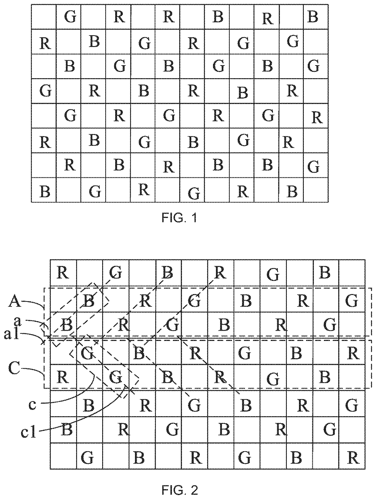
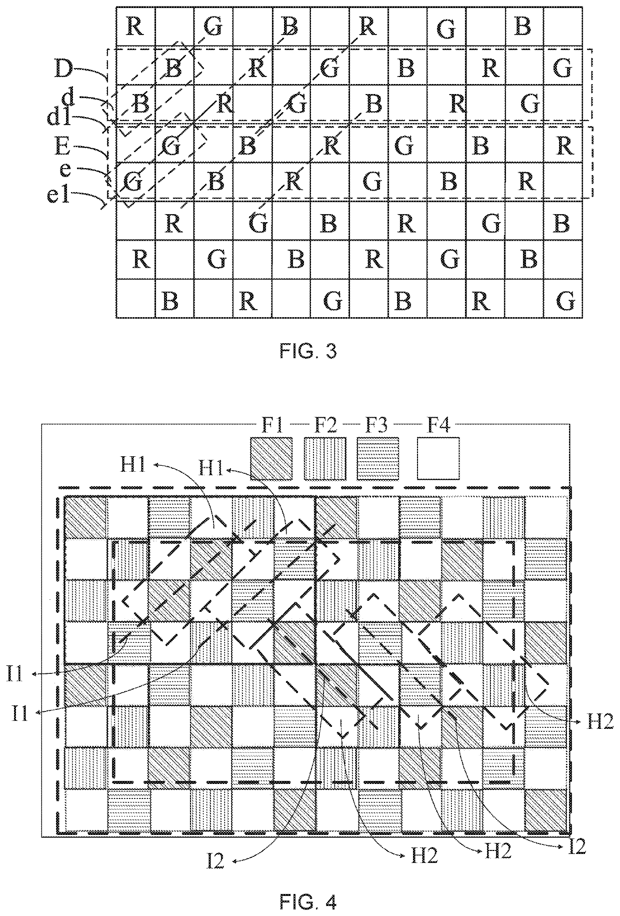
[0038]Refer to FIG. 1, a schematic diagram of a sub-pixel structure of an organic light emitting diode pixel array structure according to the present disclosure is provided. The organic light emitting diode pixel arrangement structure of the embodiment includes a central area in a middle of a display panel and an edge area located around the central area. It can be understood that a number of pixels of an actual display panel is much greater than that illustrated in FIG. 1. A shape of the display panel maybe not necessarily a regular rectangular structure. For example, in IPHONE X, four corners of the display panel are arc-shaped with a notch above. Similarly, a pixel arrangement on the actual display panel maybe not necessarily have the appearance in FIG. 1, and only an arrangement rule of each sub-pixel is illustrated here and in subsequent drawings.

[0039]The edge area may correspond to a portion where a plurality of rows or columns of sub-pixels are located around a display area ...

fourth embodiment

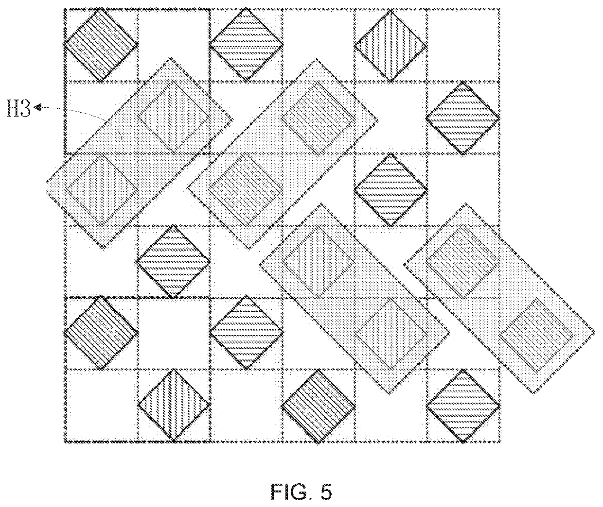
[0050]Refer to FIG. 4, a schematic diagram of a sub-pixel structure of an organic light emitting diode pixel array structure according to the present disclosure is provided. In the embodiment, the space units F4 each are disposed between every two adjacent sub-pixels on each row, and the sub-pixels on a row adjacent to a corresponding row are disposed in alignment with the space units F4 on the corresponding row, respectively. As illustrated in FIG. 4, top, bottom, left, and right directions of each sub-pixel in the central area are the space units F4. That is, the sub-pixels and adjacent sub-pixels are arranged at intervals by the space units F4.

[0051]In the central area, four sub-pixels are arranged around a corresponding sub-pixel and have at least three different colors. In the embodiment, the organic light emitting diode pixel array structure includes red sub-pixels F1, blue sub-pixels F2, and green sub-pixels F3. As illustrated in FIG. 4, red sub-pixels F1 are disposed on a to...

fifth embodiment

[0055]In the embodiment, a shape of each of the sub-pixels may be a circle, a rectangle, a square, or a diamond. Refer to FIG. 5, a schematic diagram of a sub-pixel structure of an organic light emitting diode pixel array structure according to the present disclosure is provided. Sub-pixels in the organic light emitting diode array structure of the display panel have a diamond shape.

[0056]Specific repeating pixel unit group in the organic light emitting diode pixel arrangement structure of the embodiment may be as illustrated in FIG. 4, and structure of each pixel unit group may be as follow.

[0057]In a first row, red sub-pixel F1, space unit F4, green sub-pixel F3, space unit F4, blue sub-pixel F2, and space unit F4 are arranged.

[0058]In a second row, space unit F4, blue sub-pixel F2, space unit F4, red sub-pixel F1, space unit F4, and green sub-pixel F3 are arranged.

[0059]In a third row, blue sub-pixel F2, space unit F4, red sub-pixel F1, space unit F4, green sub-pixel F3, and spac...


PUM


Abstract

An organic light emitting diode pixel arrangement structure and a display panel are provided. The organic light emitting diode pixel arrangement structure includes a central area and an edge area located around the central area. In the central area, four sub-pixels are arranged around a corresponding sub-pixel and have at least three different colors. A color of the corresponding sub-pixel is same as a color of one of the four sub-pixels arranged around the corresponding sub-pixel, so as to achieve high resolution display of the display panel.

Description

RELATED APPLICATIONS[0001]This application is a National Phase of PCT Patent Application No. PCT / CN2018 / 084717 having International filing date of Apr. 27, 2018, which claims the benefit of priority of Chinese Patent Application No. 201810090967.1 filed on Jan. 30, 2018. The contents of the above applications are all incorporated by reference as if fully set forth herein in their entirety.FIELD AND BACKGROUND OF THE INVENTION[0002]The present disclosure relates to the field of panel display technologies, and more particularly to an organic light emitting diode pixel arrangement structure and a display panel.[0003]In flat panel display technologies, organic light emitting diode (OLED) display devices have many advantages such as lightness, thinness, active light emission, fast response speed, large viewing angles, wide color gamut, high brightness, and low power consumption. The OLED display devices have gradually become the third-generation display technologies behind liquid crystal...

Claims


Application Information

Patent Timeline
Patent Type & Authority Patents(United States)
IPC IPC(8): H01L27/32
CPCH01L27/3218H10K59/353
Inventor TIAN, NIAN
Owner WUHAN CHINA STAR OPTOELECTRONICS SEMICON DISPLAY TECH CO LTD
Why Eureka
Try Eureka