Sensor apparatus and method for use in imaging features of an object

a technology of imaging features and sensors, applied in the field of sensor devices and methods for use in imaging features of objects, can solve the problems of 4) cost, 4) susceptibility to electrostatic discharge (esd), and 4) susceptibility to contamination

Inactive Publication Date: 2002-06-06
ARETE ASSOCIATES INC
View PDF0 Cites 254 Cited by
  • Summary
  • Abstract
  • Description
  • Claims
  • Application Information

AI Technical Summary

Problems solved by technology

Areas of weakness with silicon sensors are 1) ruggedness, 2) susceptibility to electrostatic discharge (ESD), 3) susceptibility to contamination, and 4) cost.
However, when using silicon sensors for measuring fingerprints, the measures used in traditional semiconductor manufacturing to mitigate such weaknesses of silicon are in conflict with optimal fingerprint imaging.
Finally, the usual method for reducing cost in silicon, reducing overall die size by scaling down the size of the components built into the silicon, cannot be used, as the performance of the sensor will be directly impacted by the total area available for capturing a fingerprint.
Thus, tradeoffs are required when making a silicon sensor for imaging a fingerprint, and these necessarily inhibit optimum sensor performance.

Method used


Image

  • Sensor apparatus and method for use in imaging features of an object
  • Sensor apparatus and method for use in imaging features of an object
  • Sensor apparatus and method for use in imaging features of an object

Examples


Embodiment Construction

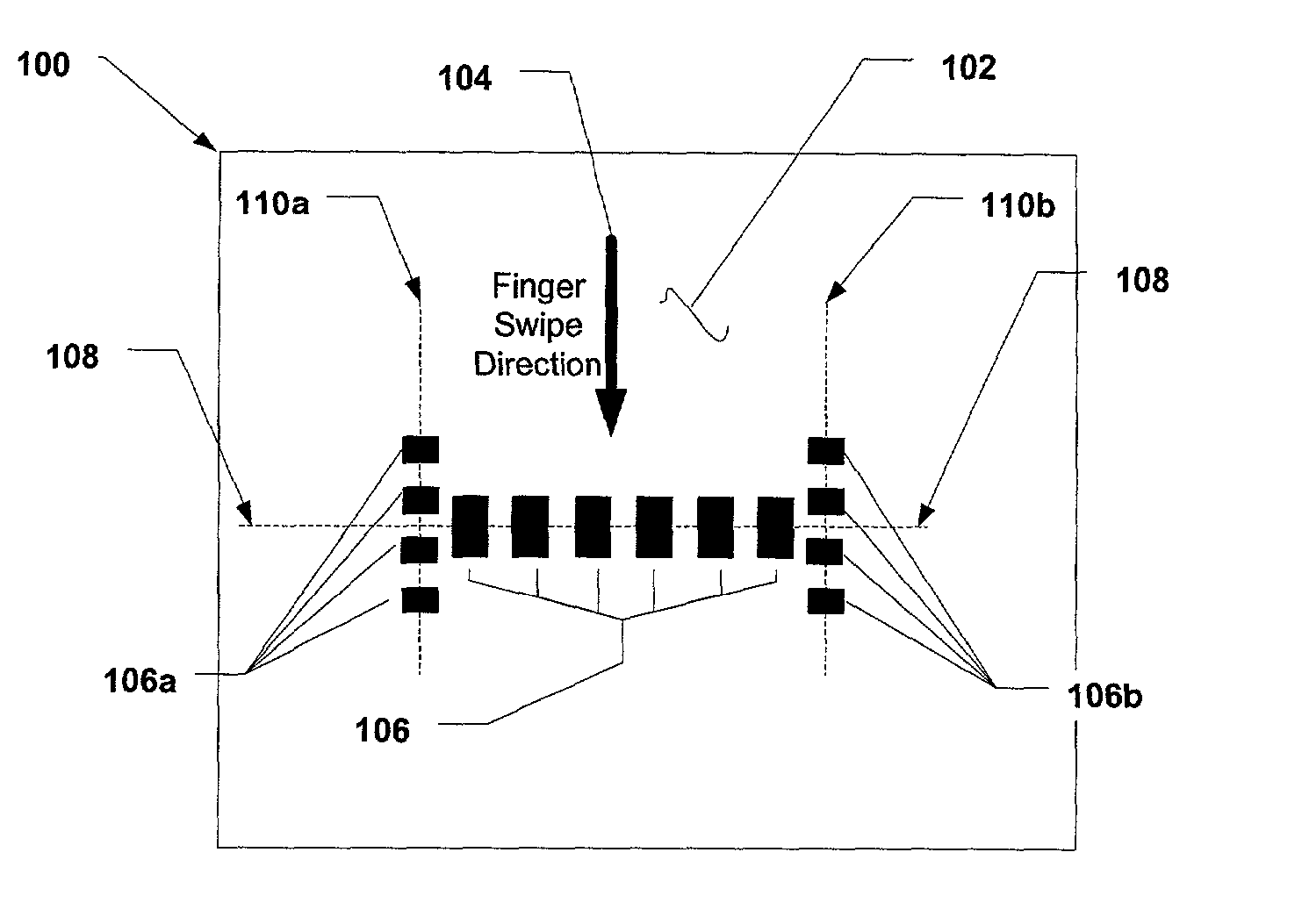
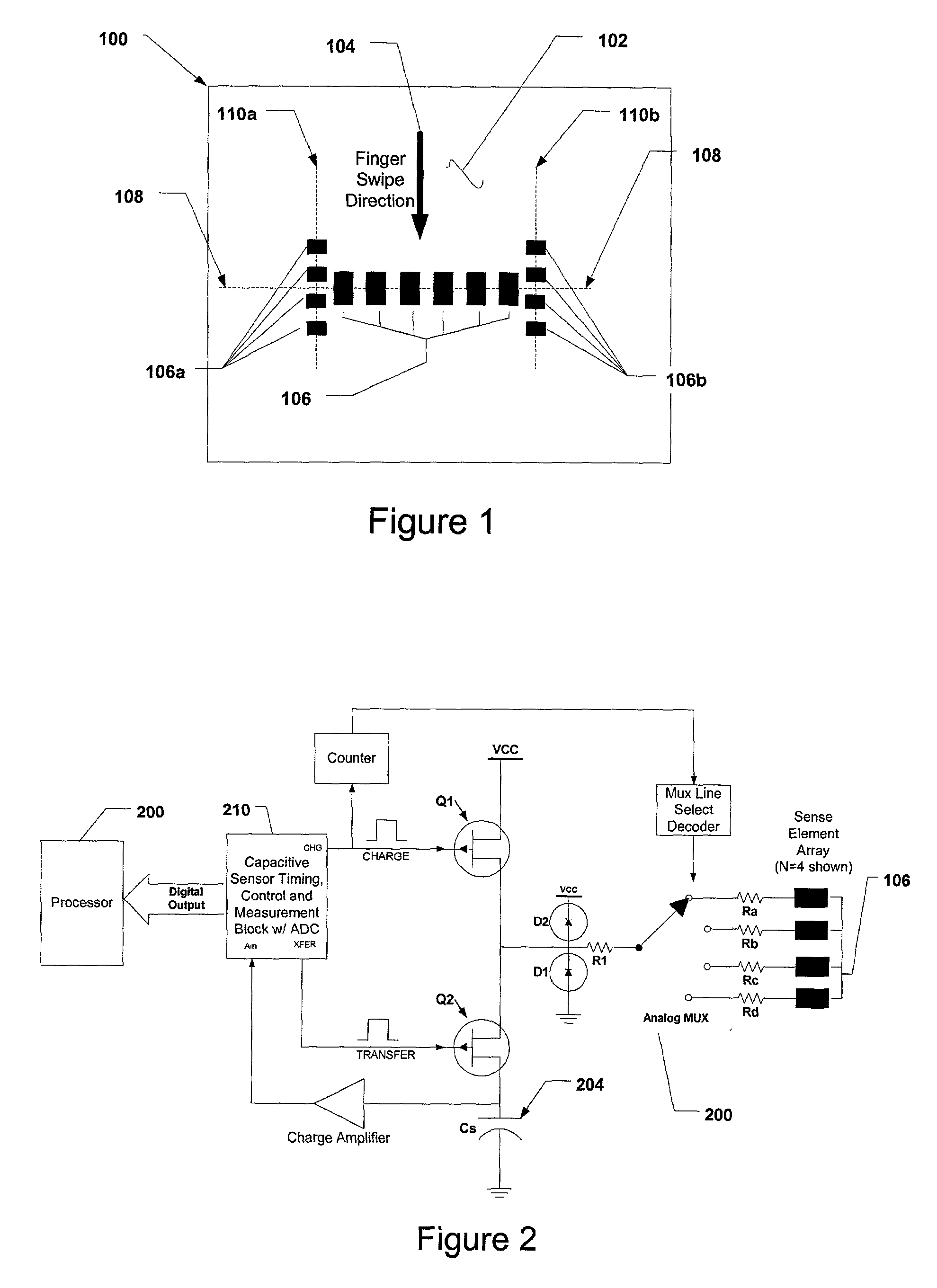
[0029] As described above, the present invention relates to a sensing device and method which is designed to be particularly useful in connection with imaging an object such as a person's fingerprint. The invention is described herein in connection with a sensor for imaging a person's fingerprint, but it will be clear to those skilled in the art that the invention can be used for various applications where it is important to sense and image an object having surface features that can be measured with such a sensor.

[0030] FIG. 1 schematically illustrates a sensor 100 constructed according to the principles of the present invention. The sensor 100 includes a surface 102 configured to enable an object such as a person's finger to slide thereon in a predetermined direction. In FIG. 1, the direction arrow 104 illustrates the direction that a person's finger would slide along the surface 102. For simplicity, the conductive PCB connections and planar (e.g., ground plane) features are not sh...


PUM


Abstract

A sensing device and method for use in imaging surface features of an object is provided. A surface along which an object can slide in a predetermined direction includes an array of contact sense elements configured to form a single array oriented transverse to the predetermined direction and at least one additional contact sense element located in spaced relation to the single array in a manner that enables a velocity measurement of the object in the predetermined direction. A scanning device is configured to provide a periodic scan of the array of contact sense elements, and a processor in circuit communication with the scanning device is configured to receive data from the scanning device and to produce image and velocity data related to the object. Preferably, the contact sense elements are electrically conductive elements disposed on a ceramic or polymeric substrate, using printed circuit board construction. A technique is described that enables the reconstruction of an object from such a device

Description

Related Application / Claim of Priority[0001] This application is related to and claims priority from Provisional Application Ser. No. 60 / 256,499, filed Dec. 5, 2000.Technical Field[0002] The present invention relates to a sensor device and method for use in imaging features of an object, e.g. a person's fingerprint.Background[0003] There are currently three major approaches to so-called live scan fingerprint readers: 1) visible light optical, 2) silicon-based capacitive sensors, and 3) silicon-based thermal-infrared (IR) sensors.[0004] The visible light optical sensors rely on the exploitation of the air-tissue index of refraction differential by imaging the finger near the critical angle for the finger placed on the imaging contact surface.[0005] The silicon-based sensors, which rely on measurements of the fingerprint capacitance as a function of location on the finger, follow one of two general approaches. One approach involves measuring the discharge behavior of an array of charge...

Claims


Application Information

Patent Timeline
Patent Type & Authority Applications(United States)
IPC IPC(8): G06K9/00
CPCG06K9/00026G06K9/0002G06V40/1335G06V40/1306
Inventor GRIFFIS, ANDREW J.
Owner ARETE ASSOCIATES INC
Why Eureka
Try Eureka