
Flash memories with adaptive reference voltages

a flash memory and reference voltage technology, applied in the field of flash memories, can solve the problems of limiting the time that data can be reliably retained in a flash memory, finite precision of read/program circuitry, and unacceptably high bit error ra

Active Publication Date: 2005-01-20
WESTERN DIGITAL ISRAEL LTD
View PDF15 Cites 299 Cited by
  • Summary
  • Abstract
  • Description
  • Claims
  • Application Information

AI Technical Summary

Benefits of technology

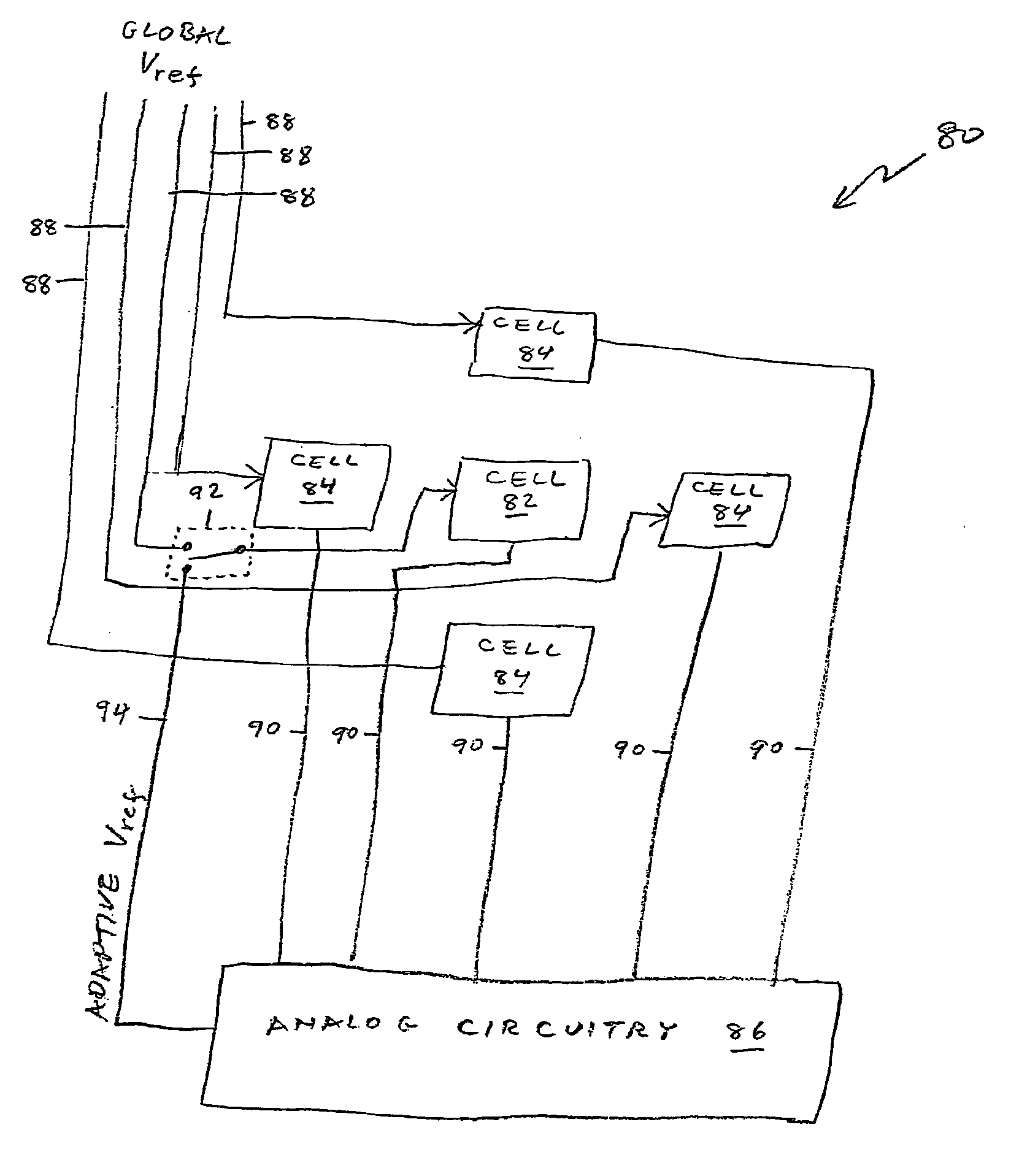
In a preferred embodiment of this aspect of the present invention, the determination of each cell's respective adaptive reference voltage(s) is based on a (preferably analog) measurement of the threshold voltages of one or more neighboring cells.
In a preferred digital embodiment of this aspect of the present invention, a preliminary estimate of each cell's threshold voltage is obtained by comparing the threshold voltage to at least one nominal reference voltage that is common to all the cells. Then, the determination of each cell's respective adaptive reference voltage(s) is based on the preliminary estimates of the threshold voltages of one or more neighboring cells. The nominal reference voltages are integral reference voltages and/or fractional reference voltages.
The scope of the present invention includes two embodiments of flash memories that use the method of the present invention for read

Problems solved by technology

The precision of the read / program circuitry is finite and is limited by random noise.
This phenomenon limits the time that data can be reliably retained in a flash memory.
A voltage band that is too narrow, relative to the associated threshold voltage distribution curve and relative to the drift of that curve over time, leads to an unacceptably high bit error rate.
Some flash technologies are unable to achieve this error rate while storing the desired number of bits per cell.

Method used


Image

  • Flash memories with adaptive reference voltages
  • Flash memories with adaptive reference voltages
  • Flash memories with adaptive reference voltages

Examples


Embodiment Construction

The present invention is a set of methods for reading flash memories more reliably than is possible according to the prior art.

The principles and operation of a flash memory according to the present invention may be better understood with reference to the drawings and the accompanying description.

Fractional Threshold Voltages

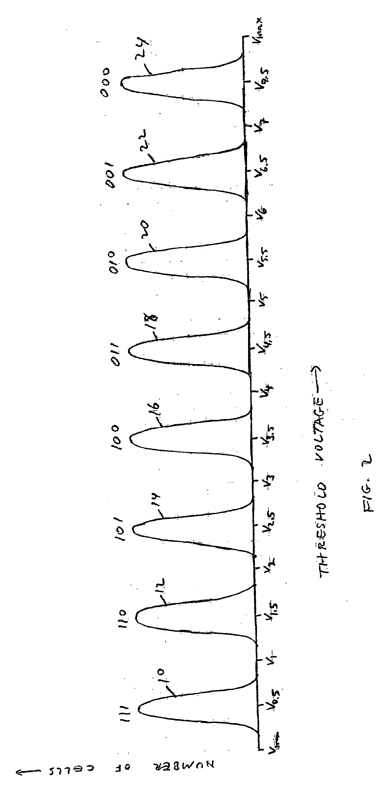
The basic innovation of the present invention is that, in addition to comparing the threshold voltages of flash cells to integral reference voltages, the threshold voltages also are compared to fractional reference voltages. Returning now to the drawings, FIG. 2 is FIG. 1 with the addition of eight fractional reference voltages, V0.5, V1.5, V2.5, V3.5, V4.5, V5.5, V6.5 and V7.5, in the centers of their respective voltage bands. In general, a flash cell for storing m bits has 2m voltage bands and so has 2m−1 integral reference voltages. For example, in the case of a type 1 flash memory whose cells are read with m comparisons of a flash cell's threshold volt...


PUM


Abstract

Cells of a flash memory are read by determining respective adaptive reference voltages for the cells and comparing the cells' threshold voltages to their respective reference voltages. The adaptive reference voltages are determined either from analog measurements of the threshold voltages of the cells' neighbors or from preliminary estimates of the cells' threshold voltages based on comparisons of the cells' threshold voltages with integral or fractional reference voltages common to all the cells. Cells of a flash memory also are read by comparing the cells' threshold voltages to integral reference voltages, comparing the threshold voltages of cells that share a common bit pattern to a fractional reference voltage, and adjusting the reference voltages in accordance with the comparisons.

Description

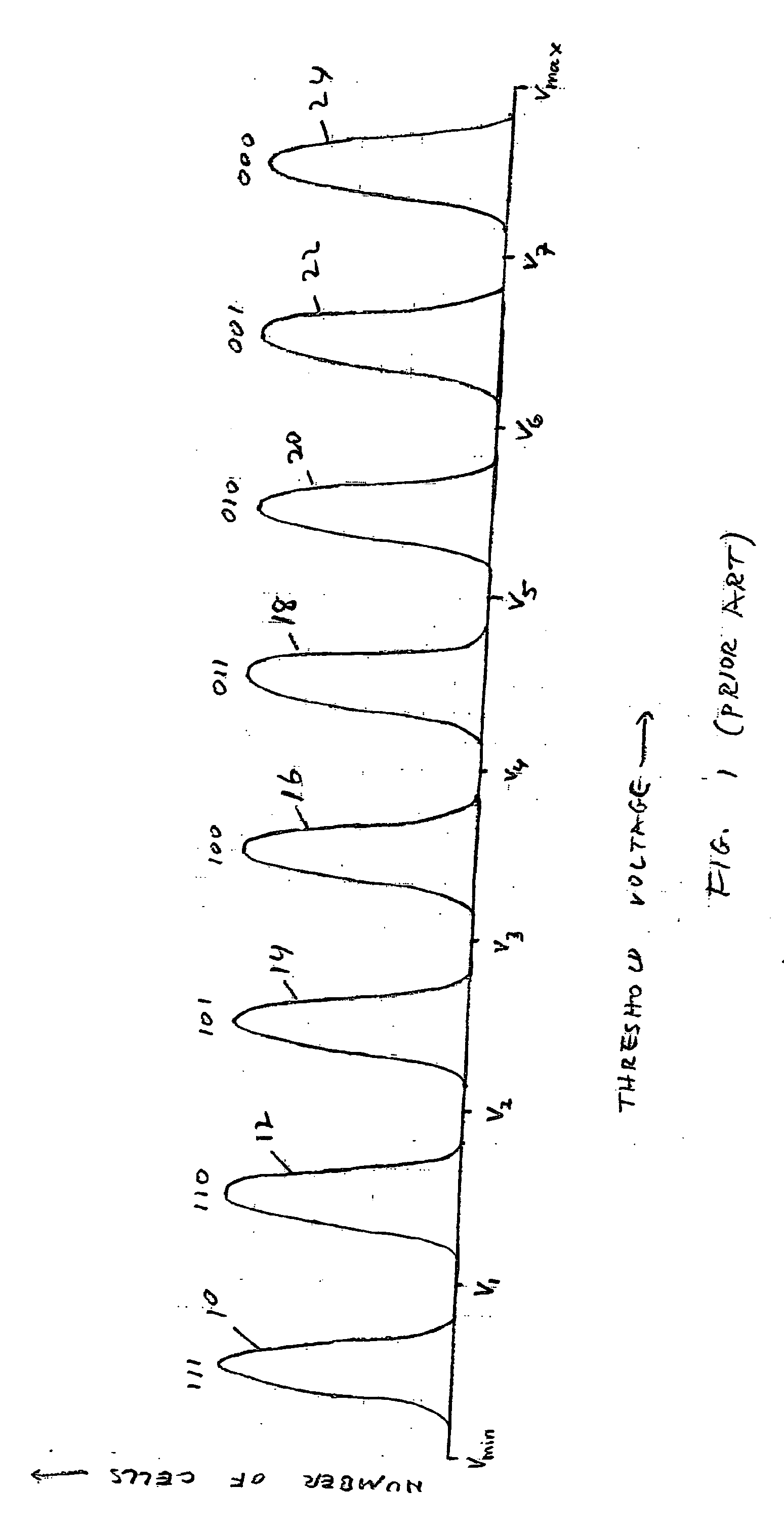
FIELD AND BACKGROUND OF THE INVENTION The present invention relates to flash memories and, more particularly, to methods for reading such memories more reliably. Originally, flash memories stored only one bit per cell. Flash memories that store two bits per cell now are available commercially, and flash memories that store more than two bits per cell are being developed. Flash memories that store one bit per cell are called “Single Level Cell” (SLC) memories. Flash memories that store more than one bit per cell are called “Multi Level Cell” (MLC) memories. FIG. 1 illustrates how a bit pattern of three bits is stored in a MLC memory that is capable of storing three bits per cell. The threshold voltage of a flash cell is in a range, called the “voltage window”, from a minimum value Vmin to a maximum value Vmax. For historical reasons, writing data to a flash cell is called “programming” the flash cell. This is done by applying voltage pulses to the cell, to inject electrons from th...

Claims


Application Information

Patent Timeline
IPC IPC(8): G11CG11C11/56G11C16/04G11C16/06
CPCG06F11/1068G11C2211/5634G11C11/5642G06F11/1072G11C16/04
Inventor BAN, AMIR
Owner WESTERN DIGITAL ISRAEL LTD
Learn More