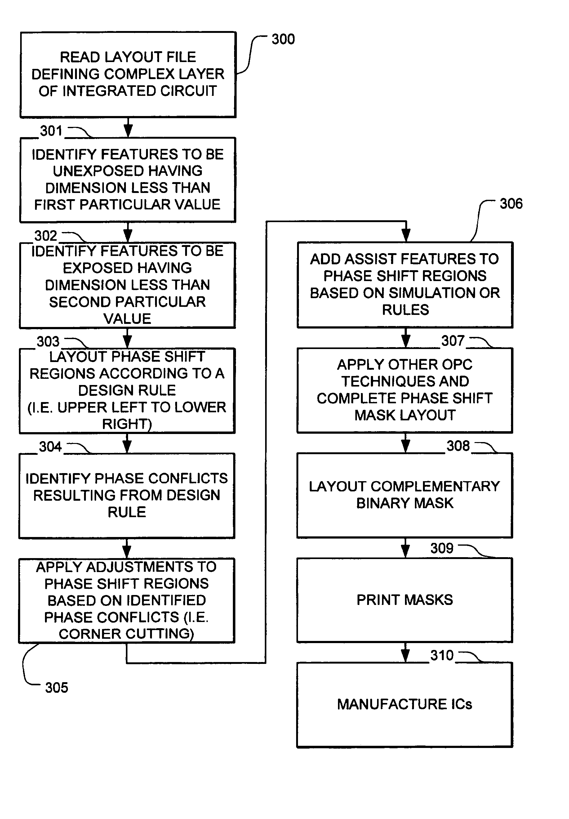
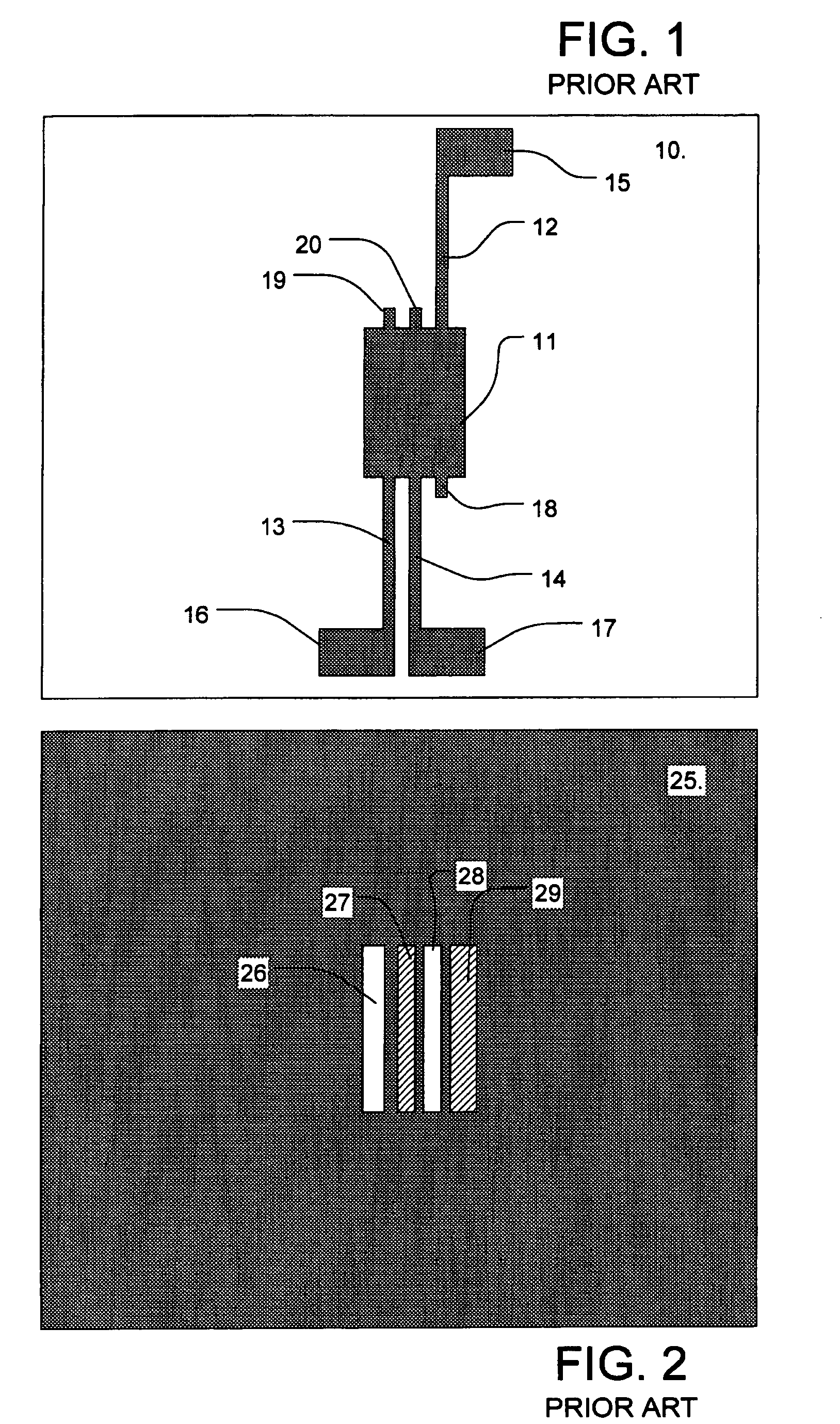
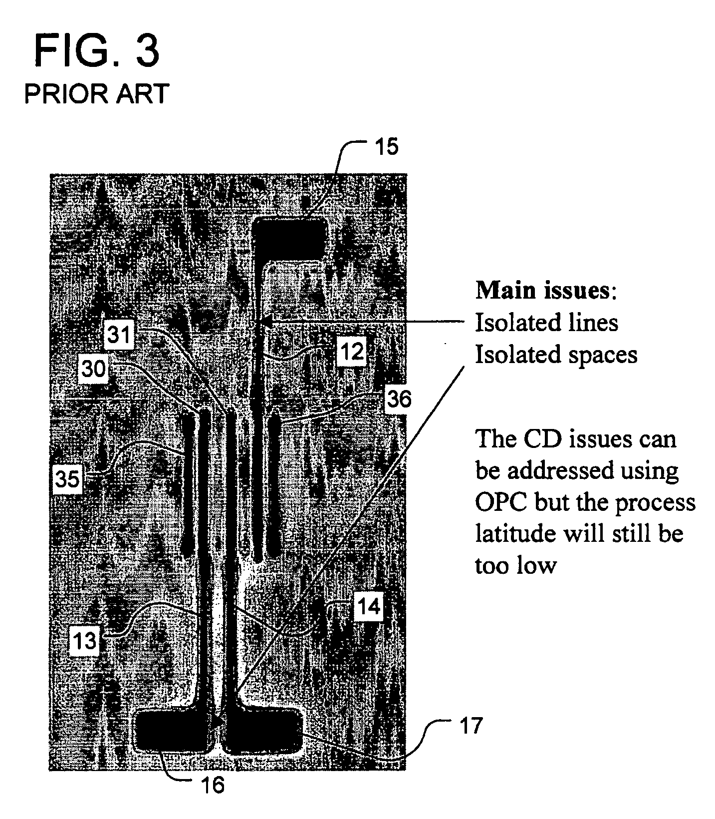
In one embodiment, the pattern to be laid out includes features having a dimension smaller than a first particular feature size (e.g., a narrow line), and at least one relatively large feature, such as a flag shaped feature. In the pattern according to this embodiment, the at least one relatively large feature and another feature (e.g. a line or another flag shaped feature) in the pattern have respective sides separated by a space between said respective sides, said space having a dimension less than a second particular feature size. Phase shift regions are laid out for the identified pattern to produce a
phase shift mask, the
phase shift mask having a first set of phase shift regions to define said features having a dimension smaller than a particular feature size, and a second set of phase shift regions to assist definition of said side of said relatively large feature.
As a result of the
layout rule, regions in the
phase shift mask may result in phase conflicts. Thus, the invention also includes applying an adjustment to one or more of the phase shift regions in the phase shift
mask to correct for phase conflicts. The adjustment in one preferred embodiment comprises dividing a phase shift region having a first phase into a first phase shift region having the first phase in a second phase shift region having the second phase. An opaque feature is added to the phase shift mask between the first and second phase shift regions. The complementary mask includes a corresponding opaque feature preventing
exposure of the features to be exposed using the first and second phase shift regions in the phase shift mask, and includes a
cut-out over the opaque feature separating the first and second phase shift regions to
expose any feature resulting from the
phase difference between the first and second phase shift regions. In one embodiment, the unique structure which results from the adjustment is laid out in the first instance to prevent phase conflicts in the
layout, and so may not be considered an “adjustment” to correct a phase conflict in the layout.
For example, phase conflicts can arise in the implementation of a pattern consisting of an intersection of an odd number of line segments. The odd number of line segments defines a plurality of corners at the intersection. In this case, phase shift regions are laid out adjacent the line segments on either side of the corner so they have the same phase, and preferably continuing around the corner in all of the plurality of corners, except one. In one excepted corner, a first phase shift region having the first phase is laid out adjacent the
line segment on one side of the corner, and a second phase shift region having the second phase is laid out adjacent the
line segment on the other side of the corner. An opaque feature is added between the first and second phase shift regions in the one corner. The complementary mask includes a corresponding opaque feature preventing
exposure of the intersecting line segments left unexposed by the phase shift mask, and includes a
cut-out over the opaque feature separating the first and second phase shift regions to
expose any feature resulting from the
phase difference in the one excepted corner between the first and second phase shift regions.
According to another aspect of the invention, the process includes adding sub-resolution assist features inside a particular phase shift region in the phase shift mask. The sub-resolution features comprise in various embodiments features inside and not contacting the perimeter of the particular phase shift region. In other embodiments, the sub-resolution features result in division of a phase shift region having a first phase into first and second phase shift regions having the same phase. An opaque feature between the first and second phase shift regions acts as a sub-resolution feature to improve the shape of the resulting exposed and unexposed regions.
The sub-resolution features do not “print” in the image being exposed, but affect the intensity profile at the
wafer level, such as by improving contrast of the image and thereby improving process
latitude, and changing the size of the printed image caused by the phase shift region in which the sub-resolution feature is laid out, such as for
optical proximity correction OPC.
A method for producing integrated circuits having improved small dimension structures includes applying a photo-sensitive material to a
wafer, exposing the photo-sensitive material using the phase shift mask implemented as described above, exposing the photo-sensitive material using the complementary mask implemented as described above, and developing the photo-sensitive material. A next process step in the method for producing integrated circuits involves the removal of material underlying the photo-sensitive material according to the resulting pattern, or addition of material over the
wafer according to the pattern resulting from the use of the phase shift and complementary masks. The resulting
integrated circuit has improved, and more uniform line widths, and improved and more uniform spaces between structures on the device. In some embodiments, the resulting
integrated circuit has intersecting lines defined with phase shift masks.

