Method and system for determining constraints for a printed circuit board design module

Inactive Publication Date: 2005-02-24
HEWLETT PACKARD DEV CO LP
View PDF19 Cites 11 Cited by
  • Summary
  • Abstract
  • Description
  • Claims
  • Application Information

AI Technical Summary

Benefits of technology

[0005] The present disclosure provides a method for generating a printed circuit board design module. The method includes compiling information that is usable to derive one of more low level details associated with a printed circuit board, determining one or more high level constraints that are usable

Problems solved by technology

The steps, however, highlight the complex and time consuming task involved in PCB design.
Unfortunately, these variables may be diffic

Method used


Image

  • Method and system for determining constraints for a printed circuit board design module
  • Method and system for determining constraints for a printed circuit board design module
  • Method and system for determining constraints for a printed circuit board design module

Examples


Embodiment Construction

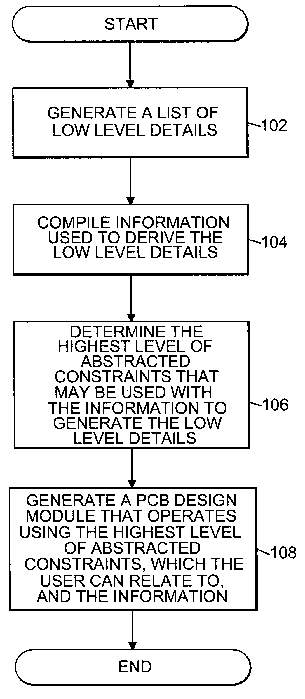
[0015] In the following detailed description of the preferred embodiments, reference is made to the accompanying drawings which form a part hereof, and in which is shown by way of illustration specific embodiments in which the invention may be practiced. It is to be understood that other embodiments may be utilized and structural or logical changes may be made without departing from the scope of the present invention. The following detailed description, therefore, is not to be taken in a limiting sense, and the scope of the present invention is defined by the appended claims.

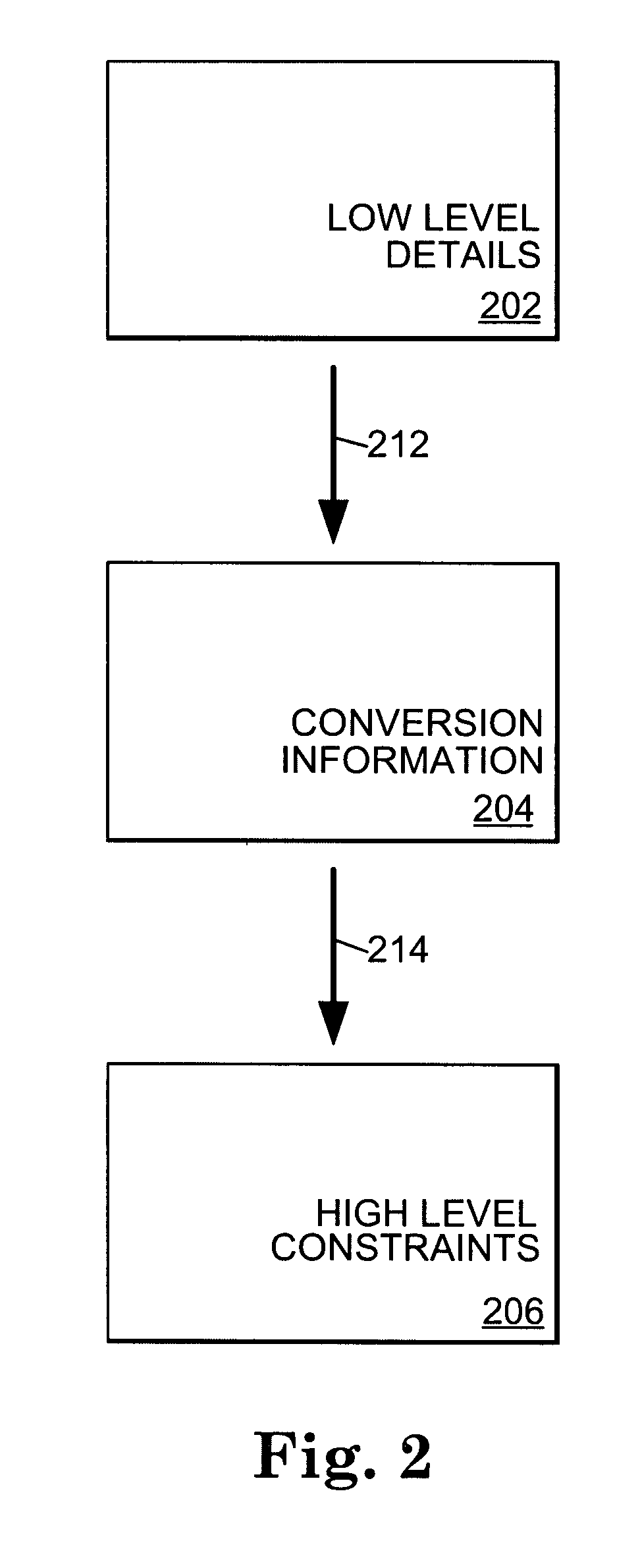
[0016] As described herein, a printed circuit board (PCB) design module is configured to receive high level constraints associated with a desired PCB from a user and generate low level details that comprise a printed circuit board design. The desired printed circuit board may be manufactured in accordance with the printed circuit board design.

[0017]FIG. 1 is a flowchart illustrating an embodiment of a method f...


PUM


Abstract

A method for generating a printed circuit board design module is provided. The method includes compiling information that is usable to derive one of more low level details associated with a printed circuit board, determining one or more high level constraints that are usable with the information to generate the low level details, and generating the printed circuit board design module such that the printed circuit board design module includes the information and such that the printed circuit board design module is configured to receive the one or more high level constraints.

Description

FIELD OF THE INVENTION [0001] The present invention generally relates to the design of printed circuit boards, and more particularly, to a method and system for determining constraints for a printed circuit board design module. BACKGROUND OF THE INVENTION [0002] A printed circuit board (PCB) is typically a thin plate on which chips and other electronic components are placed. Computers generally include one or more PCBs which are often called cards or adapters. Schematics are used by PCB designers in the PCB design process to illustrate the connections of the electrical circuits to be placed on the board. PCB designers often consider numerous design constraints correlated to the schematics in order to produce a workable PCB design. [0003] In order to convert schematics into a finished PCB layout, a process is undertaken which involves steps such as: (1) determining routing rules given impedance requirements and signal integrity issues (such as signal speed, maximum allowable cross-ta...

Claims


Application Information

Patent Timeline
IPC IPC(8): G06F17/50H03K17/693
CPCG06F17/5068G06F30/39
Inventor SWOPE, JOHN MALVERN
Owner HEWLETT PACKARD DEV CO LP
Why Eureka
Try Eureka