Solid metal block mounting substrates for semiconductor light emitting devices, and oxidizing methods for fabricating same

a technology of semiconductor light emitting devices and solid metal blocks, which is applied in the manufacture of semiconductor/solid-state devices, semiconductor devices, electrical equipment, etc., can solve the problems of failure, time-consuming and/or time-consuming, and the cost of substrates may be high,

Active Publication Date: 2005-03-10
CREELED INC
View PDF75 Cites 132 Cited by
  • Summary
  • Abstract
  • Description
  • Claims
  • Application Information

AI Technical Summary

Problems solved by technology

Unfortunately, these substrates may be costly and, in some case, more costly than the semiconductor light emitting device themselves.
Moreover, the fabrication process may also be costly, time consuming and / or subject to failures due to the number of steps therein.

Method used


Image

  • Solid metal block mounting substrates for semiconductor light emitting devices, and oxidizing methods for fabricating same
  • Solid metal block mounting substrates for semiconductor light emitting devices, and oxidizing methods for fabricating same
  • Solid metal block mounting substrates for semiconductor light emitting devices, and oxidizing methods for fabricating same

Examples


Embodiment Construction

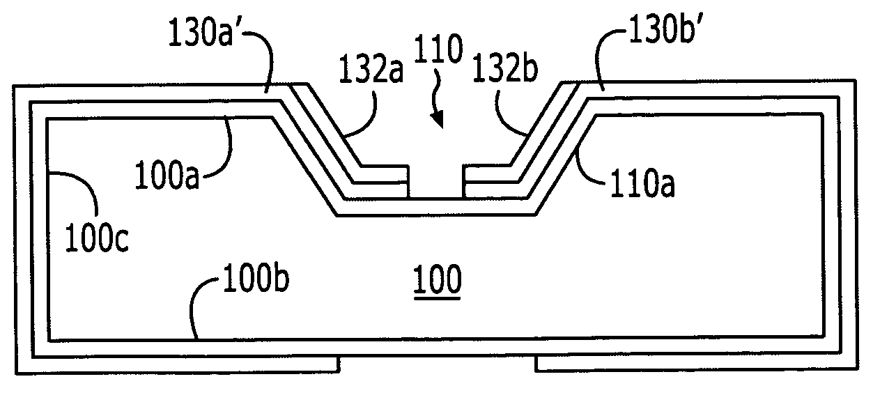
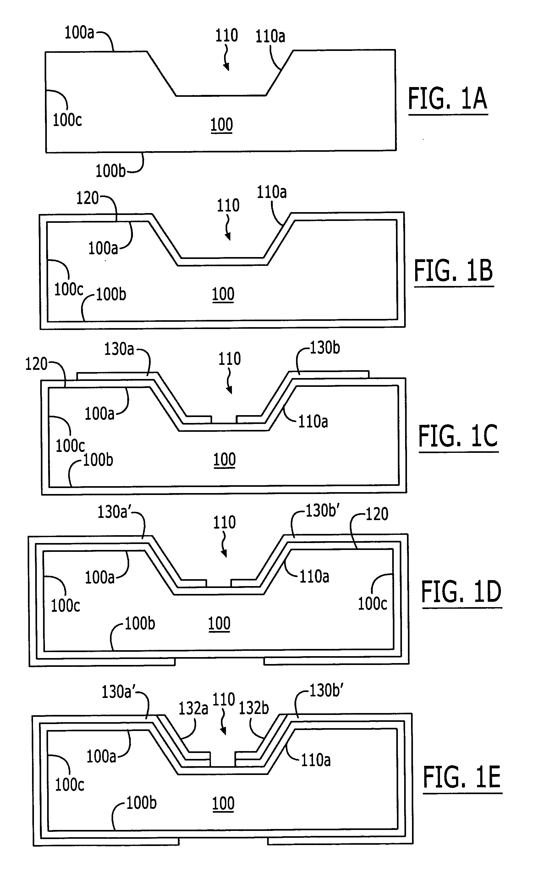
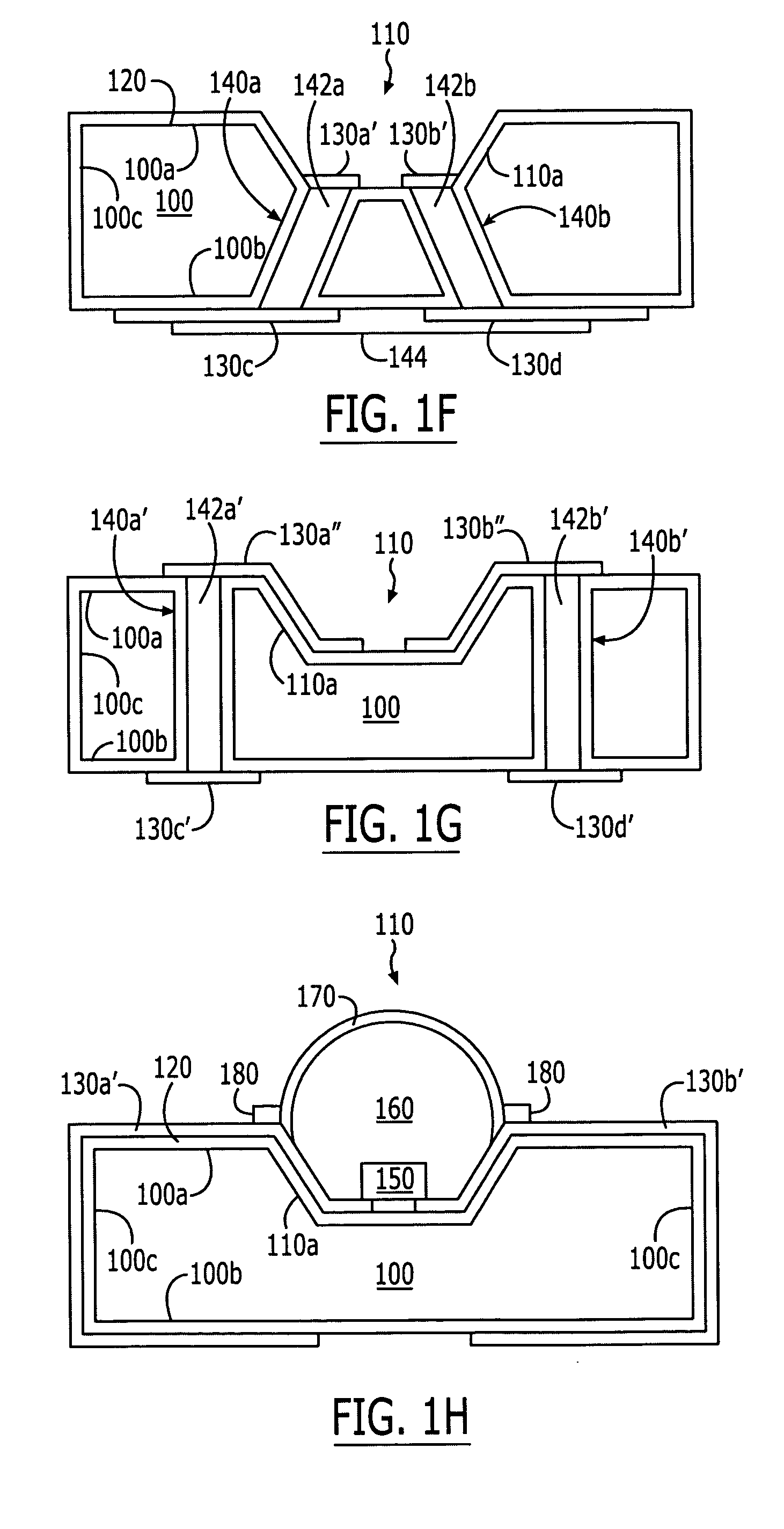
[0017] The present invention now will be described more fully hereinafter with reference to the accompanying drawings, in which embodiments of the invention are shown. This invention may, however, be embodied in many different forms and should not be construed as limited to the embodiments set forth herein. Rather, these embodiments are provided so that this disclosure will be thorough and complete, and will fully convey the scope of the invention to those skilled in the art. In the drawings, the size and relative sizes of layers and regions may be exaggerated for clarity. Like numbers refer to like elements throughout.

[0018] It will be understood that when an element such as a layer, region or substrate is referred to as being “on” another element, it can be directly on the other element or intervening elements may also be present. It will be understood that if part of an element, such as a surface of a conductive line, is referred to as “outer,” it is closer to the outside of the...


PUM


Abstract

A mounting substrate for a semiconductor light emitting device includes a solid metal block having a cavity in a face thereof that is configured for mounting a semiconductor light emitting device therein. An insulating coating is provided in the cavity, and first and second spaced apart conductive traces are provided on the insulating coating in the cavity that are configured for connection to a semiconductor light emitting device. The mounting substrate may be fabricated by providing a solid aluminum block including a cavity in a face thereof that is configured for mounting a semiconductor light emitting device therein. The solid aluminum block is oxidized to form an aluminum oxide coating thereon. The first and second spaced apart electrical traces are fabricated on the aluminum oxide coating in the cavity.

Description

FIELD OF THE INVENTION [0001] This invention relates to semiconductor light emitting devices and fabricating methods therefor, and more particularly to packaging and packaging methods for semiconductor light emitting devices. BACKGROUND OF THE INVENTION [0002] Semiconductor light emitting devices, such as Light Emitting Diodes (LEDs) or laser diodes are widely used for many applications. As is well known to those having skill in the art, a semiconductor light emitting device includes one or more semiconductor layers that are configured to emit coherent and / or incoherent light upon energization thereof. It is also known that the semiconductor light emitting device generally is packaged to provide external electrical connections, heat sinking, lenses or waveguides, environmental protection and / or other functions. [0003] For example, it is known to provide a two-piece package for a semiconductor light emitting device wherein the semiconductor light emitting device is mounted on a subst...

Claims


Application Information

Patent Timeline
Patent Type & Authority Applications(United States)
IPC IPC(8): H01L33/48
CPCH01L33/486H01L2224/48091H01L2924/00014
Inventor NEGLEY, GERALD H.LOH, BAN
Owner CREELED INC
Why Eureka
Try Eureka