Semiconductor memory device

a memory device and semiconductor technology, applied in the field of semiconductor memory devices, can solve the problems of high statistical probability of occurrence of cell defects accompanied by variations in production processes, many statistical cell defects explained above occurring at random in small units, and achieve the effect of suppressing any drop in access speed and efficient repair of defects

Inactive Publication Date: 2005-06-16
SONY CORP
View PDF11 Cites 43 Cited by
  • Summary
  • Abstract
  • Description
  • Claims
  • Application Information

AI Technical Summary

Problems solved by technology

On the other hand, however, a signal generated from a miniature memory cell becomes very weak, so the statistical probability of occurrence of cell defects accompanied with variations in the production process becomes high.
However, many statistical cell defects explained above occur at random in small units.
Therefore, too many fuses and redundant cells must be prepared with the method of using large repair units and not all of the defects can be repaired.
This does not become a major problem when there are few defects, but when a large amount of defects occur, it becomes necessary to mount a comparison circuit for each of the large number of defect addresses, so an enormous number of comparison circuits become necessary.
As a result, there is the disadvantage that the output from the defect repair memory and the comparison judgment following it are no longer in time for the access operation of the main memory.
In the technique according to Japanese Unexamined Patent Publication (Kokai) No. 11-120788, however, the memory groups (sets of the defect map storage cells and the redundant memory cells) are...

Method used


Image

  • Semiconductor memory device
  • Semiconductor memory device
  • Semiconductor memory device

Examples


first embodiment

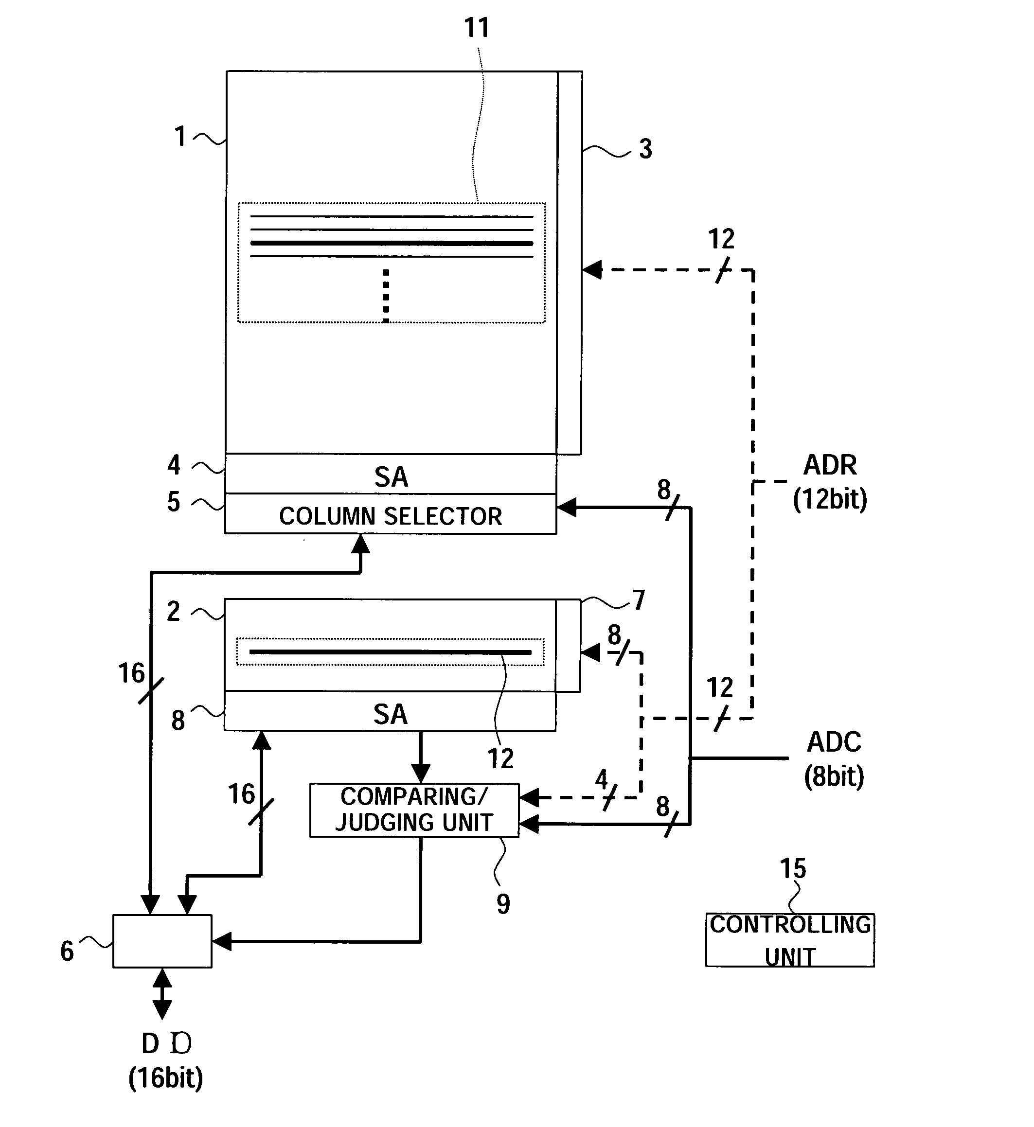
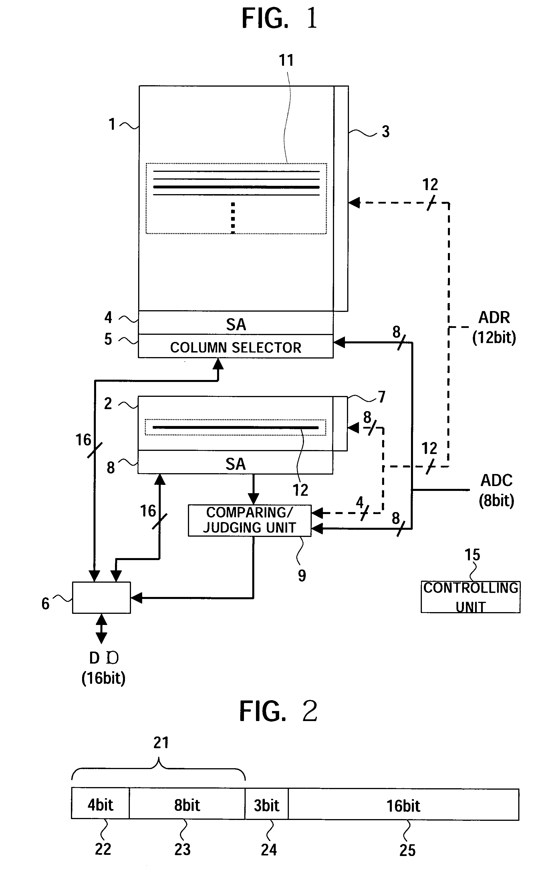
[0047]FIG. 1 is a block diagram of an example of the configuration of a semiconductor memory device according to a first embodiment of the present invention.

[0048] The semiconductor memory device illustrated in FIG. 1 has a first memory array 1 and a second memory array 2, row decoder 3 and 7, a column selector 5, sense amplifiers 4 and 8, a comparing / judging unit 9, a selector 6, and a controlling unit 15. The first memory array 1 is an embodiment of the first memory array in the first aspect of the invention. The second memory array 2 is an embodiment of the second memory array in the first aspect of the invention. The unit including the comparing / judging unit 9 and the selector 6 is an embodiment of the access switching unit in the first aspect of the invention. The controlling unit 15 is an embodiment of the controlling unit in the first aspect of the invention.

[0049] The first memory array 1 is the main memory portion of the present semiconductor memory device including usual...

second embodiment

[0094] Next, a second embodiment of the present invention will be explained.

[0095] In the semiconductor memory device shown in FIG. 1, only one memory group can be utilized for the repair of defects in each memory region (memory region of 16 word line groups 11) of the first memory array 1. Contrary to this, in the semiconductor memory device according to the present embodiment, N (N indicates a natural number of 2 or more) number of memory groups can be utilized for the repair of defects in one memory region.

[0096] The semiconductor memory device according to the present embodiment, in the same way as the semiconductor memory device shown in FIG. 1, has a first memory array 1, a second memory array 2, row decoders 3 and 7, a column selector 5, sense amplifiers 4 and 8, a selector 6, and a controlling unit 15.

[0097] However, in the present embodiment, each word line of the second memory array 2 has N number of memory groups (hereinafter referred to as a “memory set”) having the c...

third embodiment

[0114] Next, a third embodiment of the present invention will be explained.

[0115] In the semiconductor memory devices according to the first and second embodiments, when there is even 1 bit of a memory cell having a defect included in 1 word (16 bits) of memory, all memory cells of the 1 word are replaced by 1 word of the redundant memory. On the other hand, in the semiconductor memory device shown in FIG. 5 explained next, the memory cell having the defect in the 1 word is further designated by the address stored in the memory group, and this defective memory cell is replaced by 1 bit of a redundant memory cell.

[0116]FIG. 5 is a block diagram of an example of the configuration of the semiconductor memory device according to the third embodiment of the present invention. The same notations as those of FIG. 1 indicate the same components.

[0117] Namely, the semiconductor memory device illustrated in FIG. 5, in the same way as the semiconductor memory device shown in FIG. 1, has a f...


PUM


Abstract

A semiconductor memory device enabling efficient repair of defects by using limited redundant memory while suppressing a drop of access speed accompanied with the repair of defects of the memory, wherein a first memory array is divided into a plurality of memory regions for each 16 word lines and wherein defective memory addresses in regions are stored in a second memory array. When a memory address for accessing the first memory array is input, the defective memory address of the memory region including the memory to be accessed is read out from the second memory array. In this way, the addresses of defective memory in 16 word lines worth of a memory region are stored in the second memory array 2, therefore addresses of a wider range of defective memory can be stored. For this reason, it becomes possible to repair defects occurring at random efficiently.

Description

BACKGROUND OF THE INVENTION [0001] 1. Field of the Invention [0002] The present invention relates to a semiconductor memory device having the function of switching access to defective memory in a memory array to access to redundant memory provided in advance. [0003] 2. Description of the Related Art [0004] In recent years, advances in semiconductor miniaturization technology have led to remarkable advances in the increase of capacity of semiconductor memories. On the other hand, however, a signal generated from a miniature memory cell becomes very weak, so the statistical probability of occurrence of cell defects accompanied with variations in the production process becomes high. [0005] Defects of memory cells are generally dealt with by referring to a defect map describing addresses etc. of the defective cells for each repair unit. Conventionally, the defect map is programmed in fuses etc. provided inside the semiconductor memory. Defective cells and redundant cells are exchanged b...

Claims


Application Information

Patent Timeline
IPC IPC(8): G11C7/00G11C29/04G11C8/00G11C8/06G11C29/00G11C29/44
CPCG11C29/44G11C2029/1208G11C29/846G11C29/4401G11C29/00G11C8/00G11C8/06
Inventor NISHIHARA, TOSHIYUKISAKAI, YOSHIO
Owner SONY CORP
Why Eureka
Try Eureka