
Eureka
For R&D, Eureka makes reading and utilizing patents & technical documents easy.
Eureka AIR
Designed for self-driven R&D workflows. Generate viable solutions, solve complex R&D challenges, empower your innovation with AI.

Eureka Materials
Designed for material experts only. Revolutionize your material R&D, from search, analyze, to developing new materials.

TechResearch
Generate reliable direction feasibility study reports for your R&D in just a few steps.

TechSeek
Discover and master advanced knowledge NOW. Basics, ideas, possibilities, all at once.

TechMind
As an expert in R&D Theories, TechMind can generates customized viable solutions instantly.

TechRisk
Analyze your overall solution with one click, know your potential R&D risks in advance.

TechMonitor
Get weekly tech updates, stay abreast of the latest tech innovations and key insights.
Semiconductor device and method of manufacturing same, wiring board, electronic module, and electronic instrument
- Summary
- Abstract
- Description
- Claims
- Application Information
AI Technical Summary
Benefits of technology
Problems solved by technology
Method used
Image

Examples
first embodiment
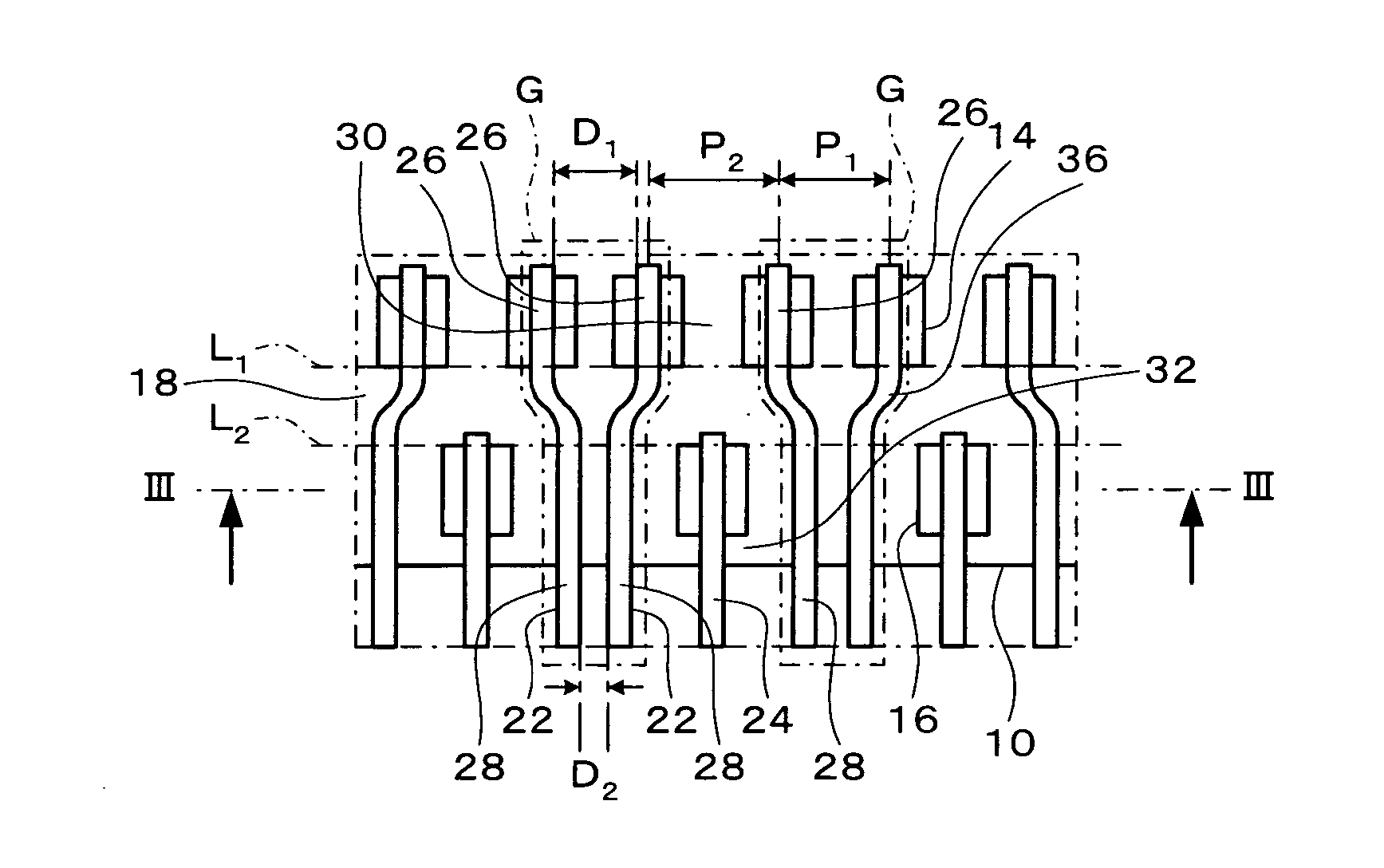
[0086] An illustrative view of a semiconductor device in accordance with a first embodiment of the present invention is shown in FIG. 1. An expanded view of the portion of the semiconductor device surrounded by a dotted line in FIG. 1 is shown in FIG. 2, and a section taken along the line III-III of FIG. 2 is shown in FIG. 3.
[0087] The semiconductor device has a semiconductor chip 10. The semiconductor chip 10 could be of a shape having rectangular surfaces (a rectangular solid shape). Integrated circuitry 12 is formed on the semiconductor chip 10. A passivation film (electrically insulating film) that is not shown in the figure is formed to cover the integrated circuitry 12.
[0088] The semiconductor chip 10 has electrodes 14 aligned along a first straight line L1. The electrodes are aligned in one line. The first straight line L1 could be a straight line that is parallel to an edge of the semiconductor chip 10 (such as a long edge of a rectangular surface thereof). A pair of regio...
second embodiment
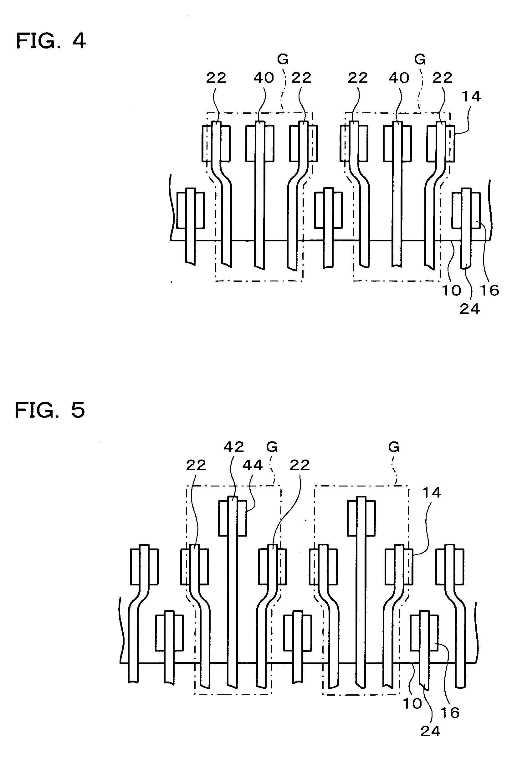
[0106] An illustrative view of a semiconductor device in accordance with a second embodiment of the present invention is shown in FIG. 6. In this embodiment, the same terminology is used as that for the first embodiment (except for the reference numbers used therefor), to correspond to the same details. In this embodiment, a pair of second leads 50 is disposed so as to sandwich each lead group G. Within each lead group G, a pair of first leads 52 on the outermost sides are formed in such a manner that a first spacing D11 is greater than a spacing D22 of the pair of second leads 50 that sandwich the lead group G (D22≦D11). In all other details, the semiconductor device, the method of manufacturing the same, and the wiring board in accordance with this embodiment correspond to those described with reference to the first embodiment and the modifications thereof.
[0107] An illustrative view of a modification of the semiconductor device in accordance with this embodiment is shown in FIG....
third embodiment
[0108] An illustrative view of a semiconductor device in accordance with a third embodiment of the present invention is shown in FIG. 8. In this embodiment, the same terminology is used as that for the first embodiment (except for the reference numbers used therefor), to correspond to the same details. In this embodiment, the plurality of lead groups comprises first lead groups G1 and second lead groups G2. The first and second lead groups G1 and G2 are disposed alternately. In other words, a pair of the second lead groups G2 is disposed so as to sandwich one of the first lead groups G1 and a pair of the first lead groups G1 is disposed so as to sandwich one of the second lead groups G2.
[0109] In this embodiment, electrodes 62 that face the second leads and are connected electrically thereto could draw a straight line L that is positioned so as to be far from an edge of a semiconductor chip 64. Second leads 60 are each disposed in such a manner that a leading end thereof (the leadi...
PUM
 Abstract
Description
Claims
Application Information
 - R&D Engineer
- R&D Manager
- IP Professional
- Industry Leading Data Capabilities
- Powerful AI technology
- Patent DNA Extraction
Browse by: Latest US Patents, China's latest patents, Technical Efficacy Thesaurus, Application Domain, Technology Topic, Popular Technical Reports.
© 2024 PatSnap. All rights reserved.Legal|Privacy policy|Modern Slavery Act Transparency Statement|Sitemap|About US| Contact US: help@patsnap.com