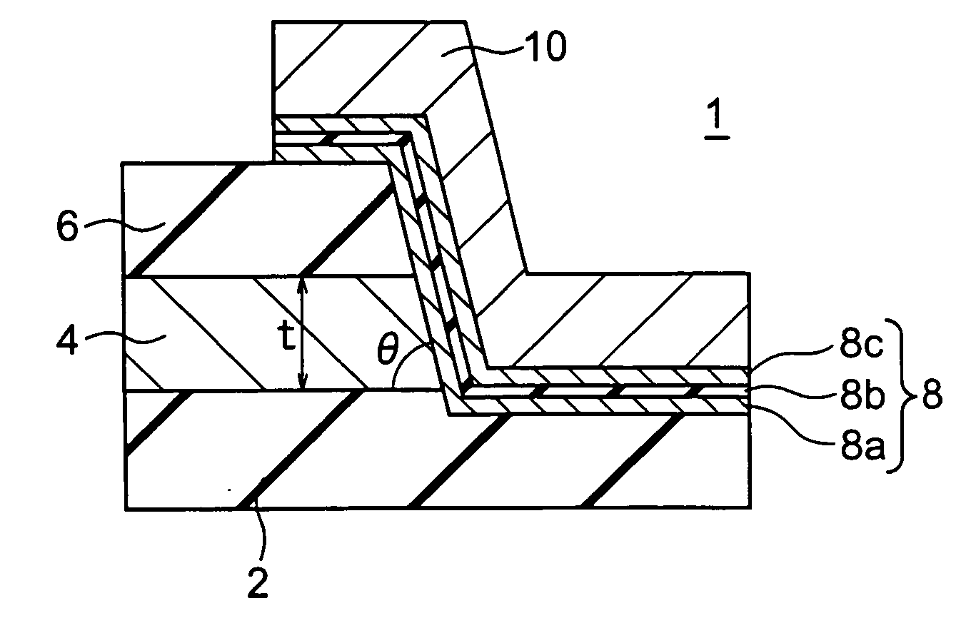
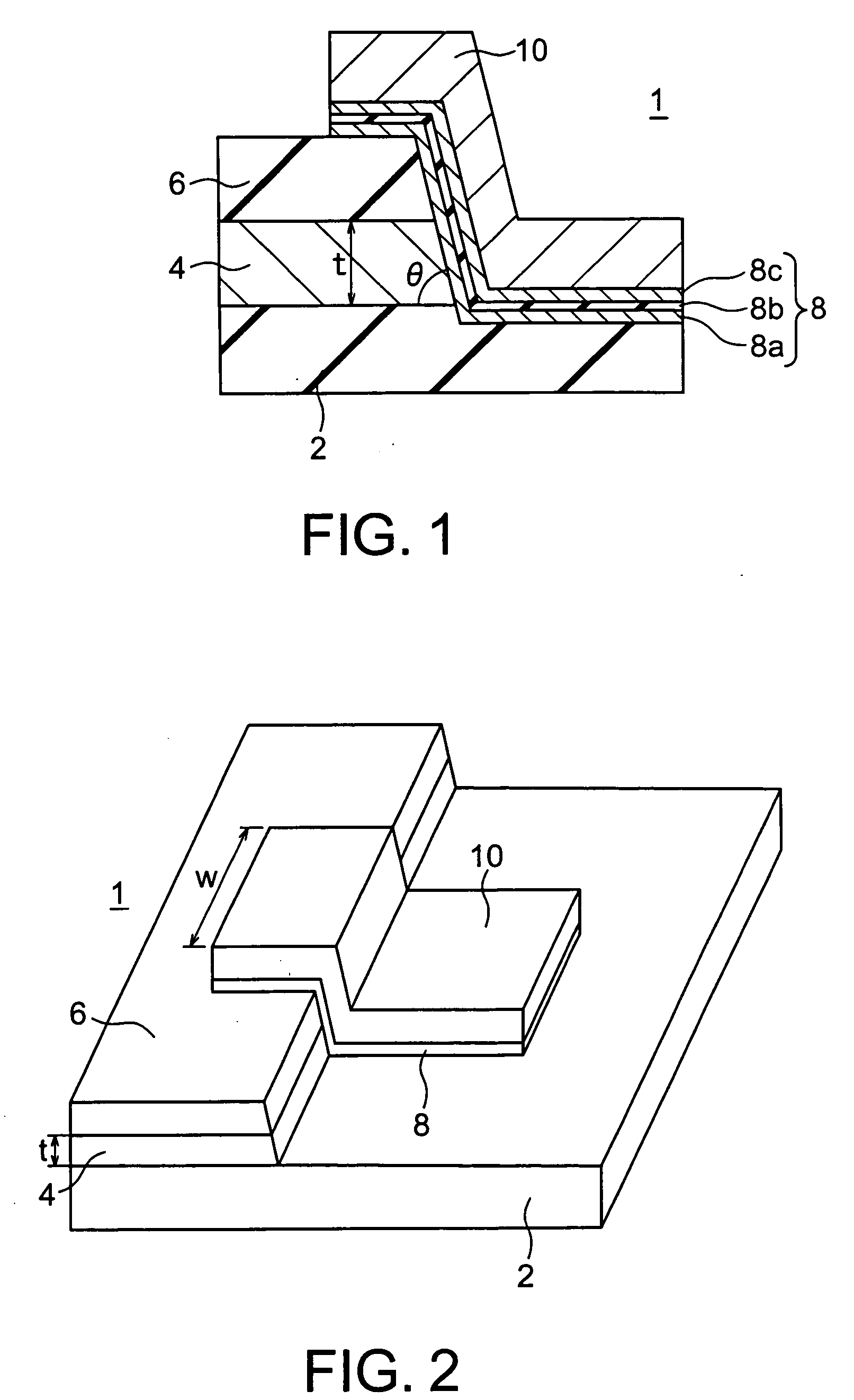
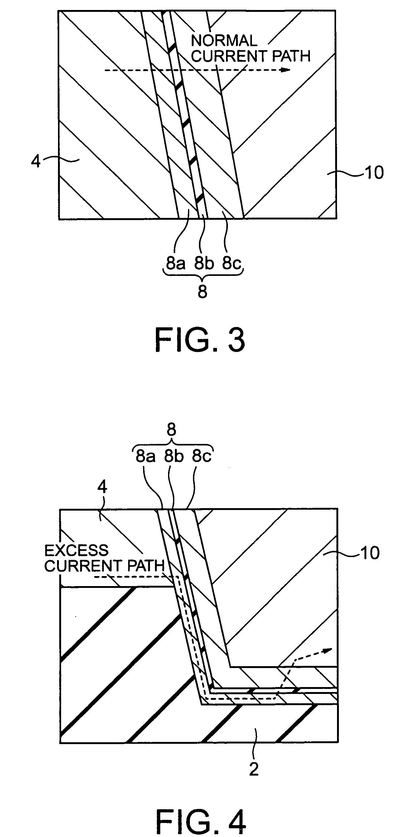
Magneto-resistance effect element and magnetic memory
a technology which is applied in the field of magnetic memory and resistance effect element, can solve the problems of inability to reduce the cell size to a dram, inability to achieve mass storage, and large power consumption
- Summary
- Abstract
- Description
- Claims
- Application Information
AI Technical Summary
Benefits of technology
Problems solved by technology
Method used
Image

Examples
seventh embodiment
(Seventh Embodiment)
[0157] Next, a magnetic memory according to a seventh embodiment of the invention will be explained with reference to FIGS. 15 and 16. FIG. 15 is a sectional view showing a constitution of a memory cell in the magnetic memory according to the embodiment, and FIG. 16 is a top view showing memory cells arranged in a column direction of the magnetic memory according to the embodiment.
[0158] The magnetic memory according to the embodiment has a plurality of bit lines BL, a plurality of word lines WL, and a plurality of memory cells arranged in a matrix. Each memory cell is provided with a magneto-resistance effect element. In the embodiment, such a constitution is employed that two adjacent memory cells constitute one pair and magneto-resistance effect elements 1a and 1b of respective memory cells share one base electrode 4. Therefore, the shared base electrode 4 is formed in an annular shape. The magneto-resistance effect element 1i (i=a, b) is provided with a TMR ...
eighth embodiment
(Eighth Embodiment)
[0161] Next, a magneto-resistance effect element according to an eighth embodiment of the invention is shown in FIG. 18. A magneto-resistance effect element 1 in the embodiment has such a constitution that layer arrangement in the TMR film 8 is reversed regarding that in the magneto-resistance effect element in the first embodiment shown in FIG. 1, namely, the ferromagnetic layer coming in contact with the base electrode layer 8c is arranged as the magnetic recording layer 4, and grain boundaries (shown with a broken line in FIG. 18) are formed in the magnetic recording layer 8c by adding non-magnetic elements (for example, Cr or Pt) into the magnetic recording layer 8c. The magnetic recording layer 8c may be made from ferromagnetic material including non-magnetic element, for example, CoCrPt, CoFeCrPt or the like.
[0162] In the embodiment, since the grain boundaries are formed in the magnetic recording layer 8c, small magnetic domains are formed in the magnetic r...
ninth embodiment
(Ninth Embodiment)
[0166] Next, a magneto-resistance effect element according to a ninth embodiment of the invention is shown in FIG. 19. A magneto-resistance effect element 1 according to the embodiment has such a constitution that a plurality of insulators 8d are provided so as to be separated from one another between the tunnel barrier layer 8b and the magnetization pinned layer 8a in the magneto-resistance effect element according to the eighth embodiment shown in FIG. 18. That is, in the embodiment, the TMR film 8 is constituted of the magnetic recording layer 8c, the tunnel barrier layer 8b, the plurality of insulators 8d, and the magnetization pinned layer 8a.
[0167] Since the plurality of insulators 8d are separately provided between the tunnel barrier layer 8b and the magnetization pinned layer 8a, a film thickness of the tunnel barrier between magnetic recording layer 8c and the magnetization pinned layer 8a is a film thickness of the tunnel barrier layer 8b in a region whe...
PUM
| Property | Measurement | Unit |
|---|---|---|
| thickness | aaaaa | aaaaa |
| current | aaaaa | aaaaa |
| thickness | aaaaa | aaaaa |
Abstract
Description
Claims
Application Information
 - R&D Engineer
- R&D Manager
- IP Professional
- Industry Leading Data Capabilities
- Powerful AI technology
- Patent DNA Extraction
Browse by: Latest US Patents, China's latest patents, Technical Efficacy Thesaurus, Application Domain, Technology Topic.
© 2024 PatSnap. All rights reserved.Legal|Privacy policy|Modern Slavery Act Transparency Statement|Sitemap