Eureka AIR delivers breakthrough ideas for toughest innovation challenges, trusted by R&D personnel around the world.

Easy axis magnetic amplifier

Inactive Publication Date: 2005-06-02
IBM CORP
View PDF4 Cites 119 Cited by
  • Summary
  • Abstract
  • Description
  • Claims
  • Application Information

AI Technical Summary

Benefits of technology

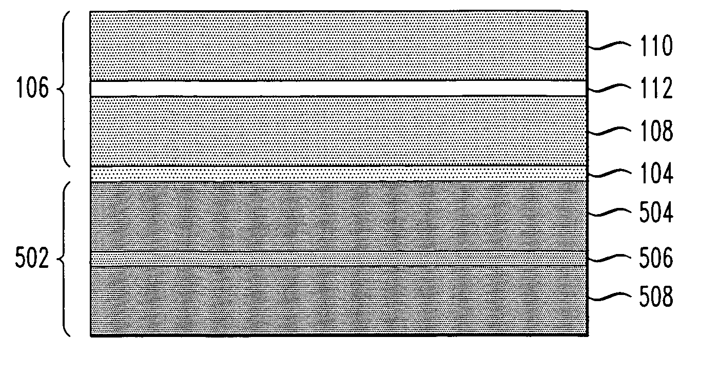
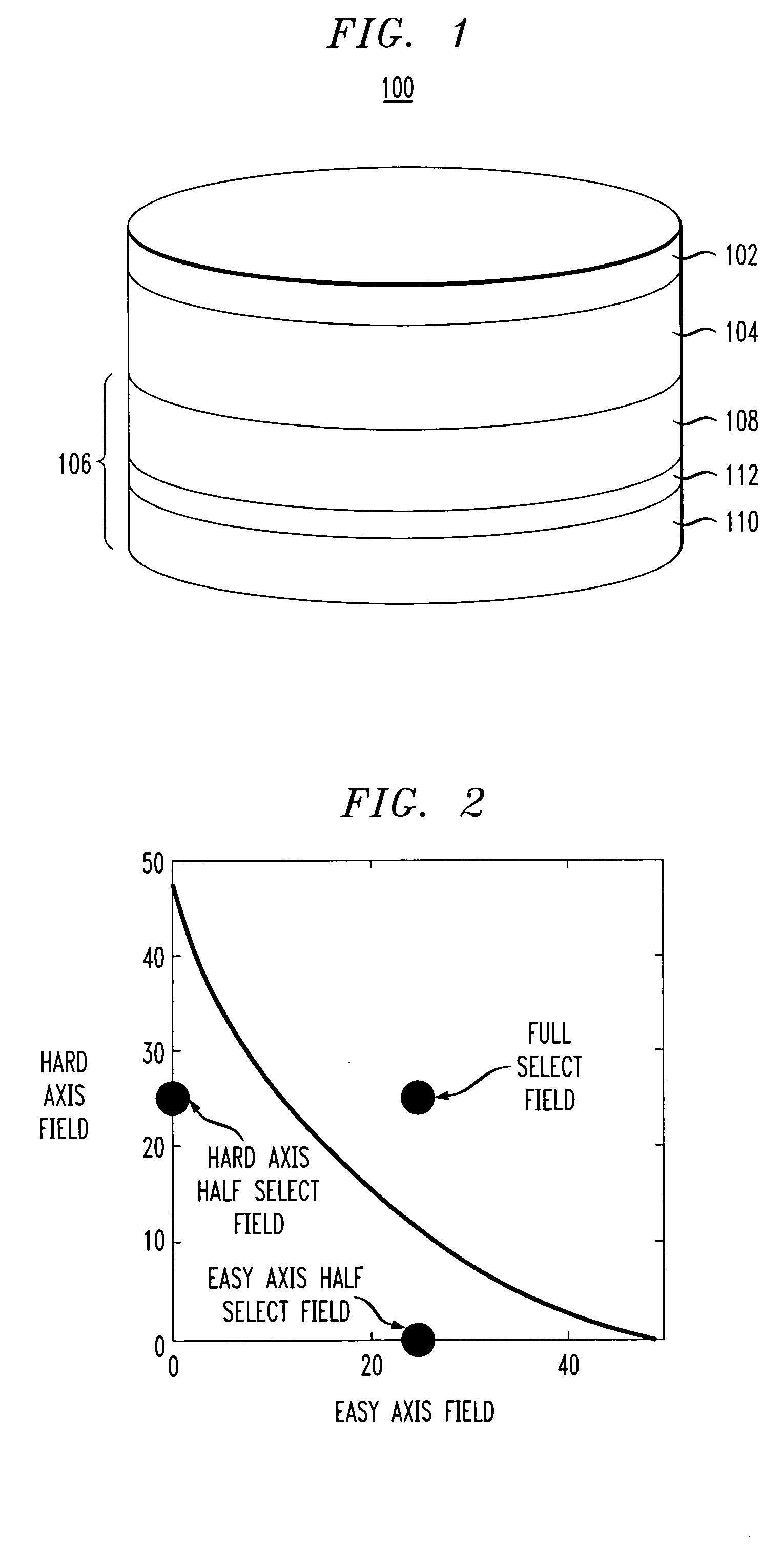
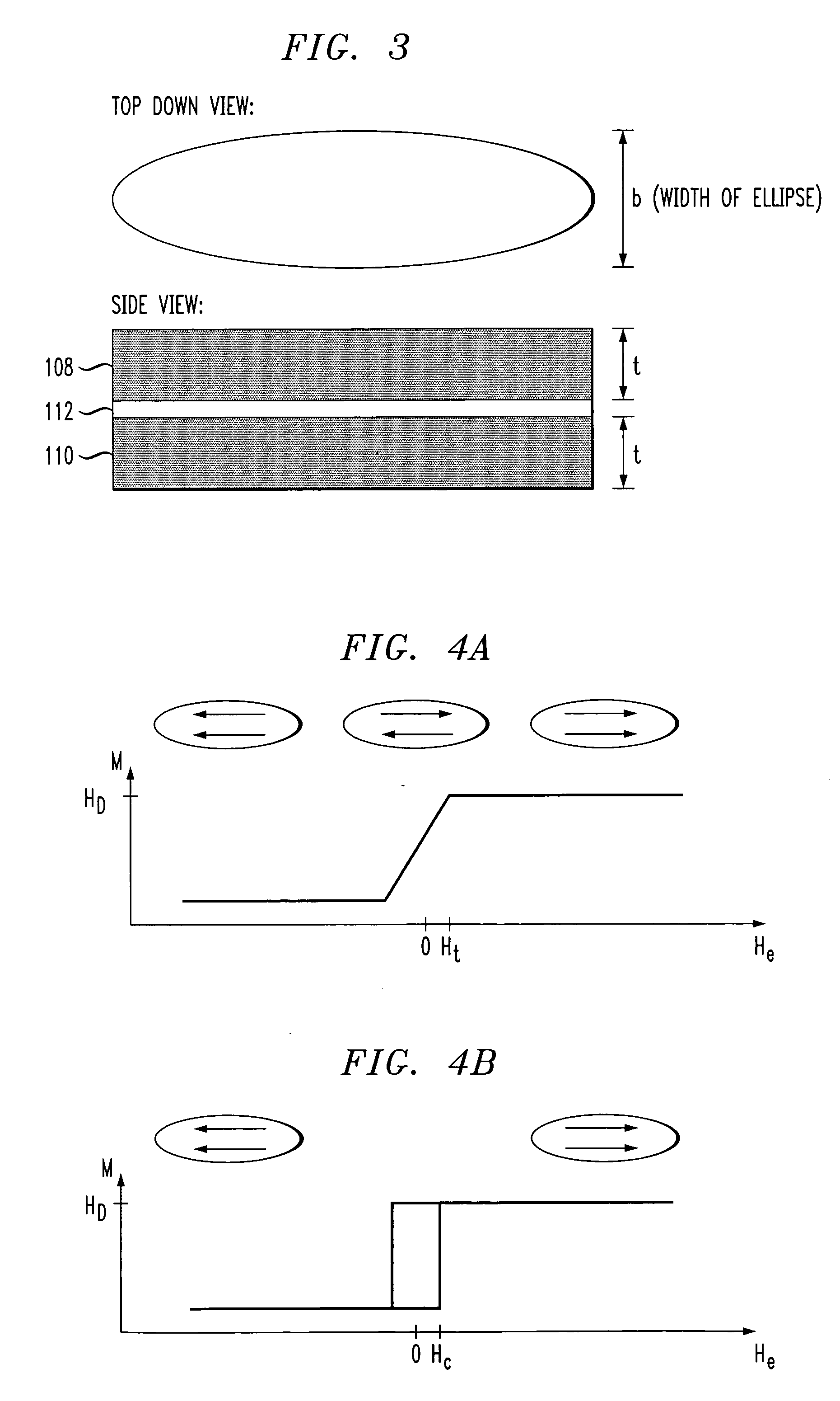
[0007] The present invention provides techniques for improved semiconductor device performance. In one aspect of the invention, a semiconductor device is provided. The device comprises at least one free magnetic layer, and a magnetic amplifier interacting with the free magnetic layer comprising two or more magnetic layers with at least one nonmagnetic layer therebetween. The nonmagnetic layer may be configured to provide parallel exchange coupling J of the magnetic layers in a range of 0<J<4⁢π⁢ ⁢t2⁢MS2⁢nyb, the magnetic layers having a long axis and a short axis, wherein t is a thickness of each magnetic layer, Ms is magnetization, ny is a demagnetizing factor defined along the short axis of the magnetic layer and b is a diameter along the short axis of the magnetic layers.

Problems solved by technology

However, during actual operation of an MRAM device, factors, such as variations in the device, cause some of the half selected cells to be arbitrarily switched, placing the reliability and validity of the stored data in question.

Method used


Image

  • Easy axis magnetic amplifier
  • Easy axis magnetic amplifier
  • Easy axis magnetic amplifier

Examples


example 1

[0048]FIG. 8 shows an illustrative astroid calculated using the single domain theory for an exemplary composite semiconductor device structure. The composite semiconductor device structure comprised a free layer consisting of a single thin layer (1.5 nanometers (nm)) with a large amount of intrinsic anisotropy (80 Oersteds (Oe)). The amplifier is composed of two layers, each four nm thick, weakly coupled together by parallel exchange coupling. The astroid shows the expected L-shaped behavior.

example 2

[0049]FIG. 9 shows an illustrative astroid calculated using the single domain theory for another exemplary composite semiconductor device structure. This structure has a free layer comprising two magnetic layers (1.5 nm and 1.6 nm thick) strongly anti-parallel coupled together, each with two Oe of intrinsic anisotropy. This configuration effectively creates a free layer with a net thickness of only 0.1 nm and a large intrinsic anisotropy of 2*(1.6+1.5) / (1.6−1.5)=62 Oe. The amplifier employed has the same configuration as that in the structure of FIG. 8, above.

example 3

[0050]FIG. 10 shows an illustrative astroid calculated using the single domain theory for another exemplary composite semiconductor device structure. Here, the same amplifier as that described in conjunction with the description of FIG. 8, above, is employed. Here the free layer is a single layer, four nm thick, with an intrinsic anisotropy of 94 Oe. At large hard axis fields, the astroid is shown to close up again. This is due to canting of the amplifier structure by the dipole field of the free layer, an effect that was ignored in the discussion above. This closing up of the astroid provides even larger write margins by allowing even larger hard axis half select fields, without switching. In order to take advantage of this feature most effectively, the hard axis field should be removed first. This is shown in FIG. 10. The easy and hard axis fields can be applied in any order. It does not matter if the hard axis field is set to a value larger than the closed region, as shown by the...


PUM


Abstract

Techniques for improved semiconductor device performance are provided. In one aspect, a semiconductor device is provided. The device comprises at least one free magnetic layer, and a magnetic amplifier interacting with the free magnetic layer comprising two or more magnetic layers with at least one nonmagnetic layer therebetween. The nonmagnetic layer may be configured to provide parallel exchange coupling J of the magnetic layers in a range of 0<J<4⁢π⁢ ⁢t2⁢MS2⁢nyb,the magnetic layers having a long axis and a short axis, wherein t is a thickness of each magnetic layer, Ms is magnetization, ny is a demagnetizing factor defined along the short axis of the magnetic layers and b is a diameter along a short axis of the magnetic layers. A method for switching a semiconductor device having at least one free magnetic layer is also provided.

Description

FIELD OF THE INVENTION [0001] The present invention relates to semiconductor devices and, more particularly, to techniques for improving semiconductor device performance. BACKGROUND OF THE INVENTION [0002] Semiconductor devices, i.e., magnetic random access memory (MRAM) devices use magnetic memory cells to store information. A cell is typically a submicron piece of magnetic material. The magnetic memory cell may be an ellipse, having the dimensions, e.g., of 300 nanometers (nm) by 600 nm in area and five nm thick. [0003] Information is stored in the device as the direction of the magnetization of a free layer in the magnetic memory cell, pointing either right or left, to store either a “1” or a “0.” When the cell is sitting in a zero applied magnetic field, the magnetization of the cell is stable, pointing either right or left. The application of a magnetic field can switch the magnetization of the free layer from right to left, and vice versa, to write information to the cell. [00...

Claims


Application Information

Patent Timeline
IPC IPC(8): G11C11/15
CPCG11C11/15
Inventor WORLEDGE, DANIEL CHRISTOPHER
Owner IBM CORP
Why Eureka
Eureka Blog
Learn More