

Introduction of metal impurity to change workfunction of conductive electrodes
a technology of conductive electrodes and impurities, applied in the field of semiconductor structures, to achieve the effect of improving the performance of a semiconductor devi
- Summary
- Abstract
- Description
- Claims
- Application Information
AI Technical Summary
Benefits of technology
Problems solved by technology
Method used
Image

Examples
Embodiment Construction
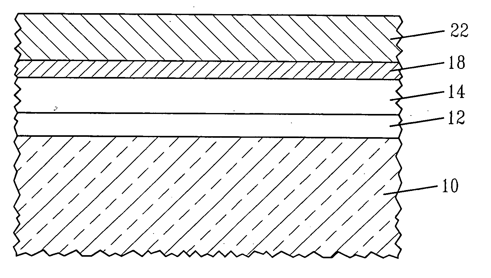
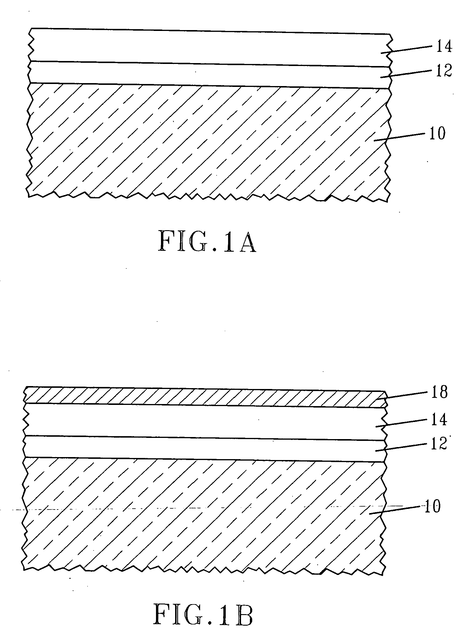
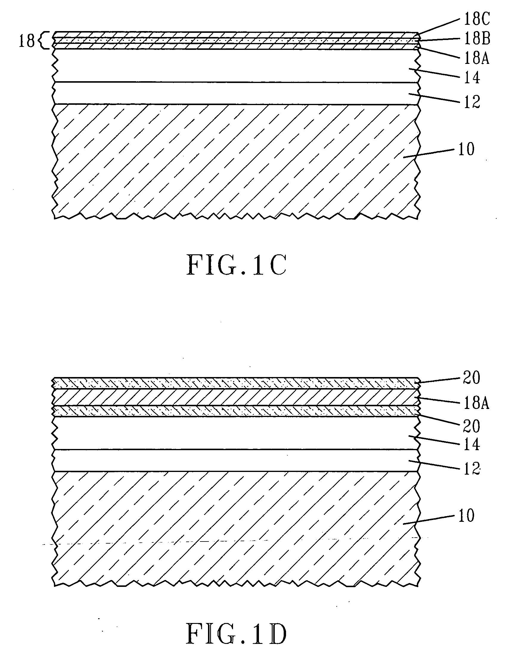
[0019] The present invention, which provides a semiconductor structure in which the workfunction of a conductive electrode stack is changed by introducing a metal impurity into a metal-containing material layer of the gate stack as well as a method of forming the same, will now be described in greater detail by referring to the following discussion and drawings that accompany the present application. It is noted that the drawings of the present application are provided for illustrative purposes and, as such, they are not drawn to scale. Also, like and / or corresponding elements are referred to herein using like reference numerals.
[0020] It is again emphasized that prior art Si MOSFETs fabricated with hafnium oxide as the gate dielectric suffer from a non-ideal threshold voltage when n-MOSFETs are fabricated. When the stacks consist of HfO2 as the dielectric, and TiN / polysilicon as the gate stack, the long channel nFET threshold voltage is in the range of 0.45 to 0.7 V range typicall...
PUM
| Property | Measurement | Unit |
|---|---|---|
| dielectric constant | aaaaa | aaaaa |
| dielectric constant | aaaaa | aaaaa |
| threshold voltage | aaaaa | aaaaa |
Abstract
Description
Claims
Application Information